

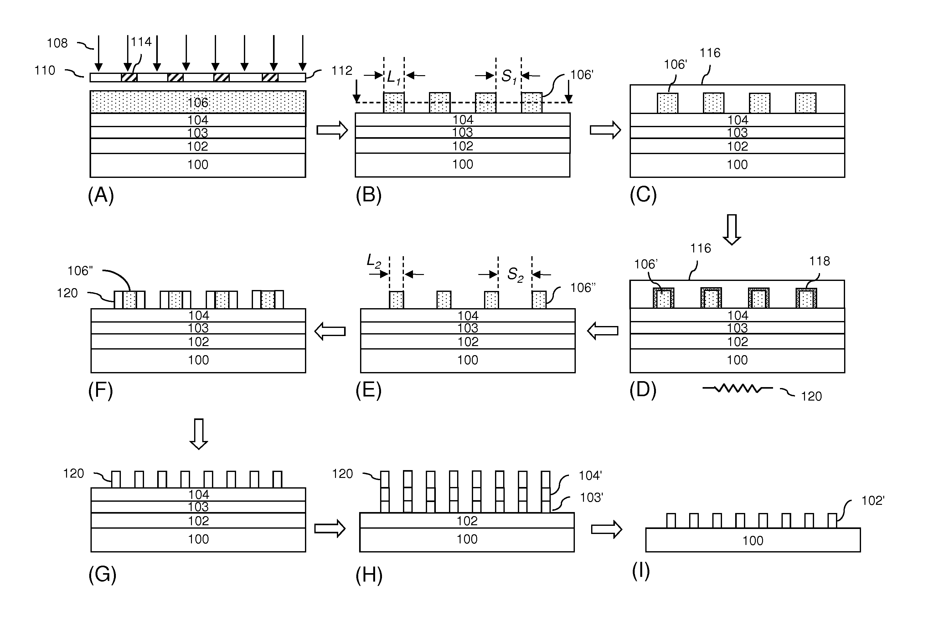
Photoresist pattern trimming methods
a technology of photoresist and pattern, applied in the field of electronic device manufacturing, can solve the problems of inability to achieve a good process window for isolated lines and posts through direct lithographic imaging, and the difference in solubility characteristics between exposed and unexposed regions of resist, so as to achieve a significant improvement of the process window for the formation of patterns such as isolated lines and posts
- Summary
- Abstract
- Description
- Claims
- Application Information
AI Technical Summary
Benefits of technology
Problems solved by technology
Method used
Image

Examples
example 1
PTC 1
[0044]2.726 copolymer of t-butyl acrylate / methacrylic acid (7 / 3 of mole ratio), 0.170 g of perfluorobutane sulfonic acid, 19.42 decane and 77.68 2-methyl-1-butynol were mixed until all components were dissolved. The resulting mixture was filtered with a 0.2 micron Nylon filter.
example 2
PTC 2
[0045]3.271 g polymer P1, 2.1808 g polymer P2, 0.348 g perfluorobutane sulfonic acid, 56.52 g 4-methyl-2-pentynol and 37.68 g di(isopentyl)ether were mixed until all components were dissolved. The resulting mixture was filtered with a 0.2 micron Nylon filter.
example 3
PTC 3
[0046]13.5 g polyacrylic acid, 1.5 g trifluoromethylbenzyl sulfonic acid (TFMBSA) and 85 g water were mixed until all components were dissolved. The resulting mixture was filtered with a 0.2 micron nylon filter.
PUM
 Abstract
Description
Claims
Application Information