Boundary-Modulated Nanoparticle Junctions And A Method For Manufacture Thereof

a technology of boundary-modulated nanoparticles and junctions, which is applied in the direction of nanotechnology, electrical equipment, semiconductor devices, etc., can solve the problem of large breakdown voltage of junctions

Inactive Publication Date: 2013-07-11
UNIV OF CONNECTICUT
View PDF1 Cites 3 Cited by
  • Summary
  • Abstract
  • Description
  • Claims
  • Application Information

AI Technical Summary

Benefits of technology

[0009]It should further be appreciated that at least a subset of the nanoparticles may include nanohelix structures. The nanohelix structures may provide an electrical tuning b...

Problems solved by technology

The nanoparticles are fabricated via a hydrothermal or solvothermal synthesis and a g...

Method used


Image

  • Boundary-Modulated Nanoparticle Junctions And A Method For Manufacture Thereof
  • Boundary-Modulated Nanoparticle Junctions And A Method For Manufacture Thereof
  • Boundary-Modulated Nanoparticle Junctions And A Method For Manufacture Thereof

Examples


Embodiment Construction

[0048]A description of example embodiments follows.

[0049]System Overview:

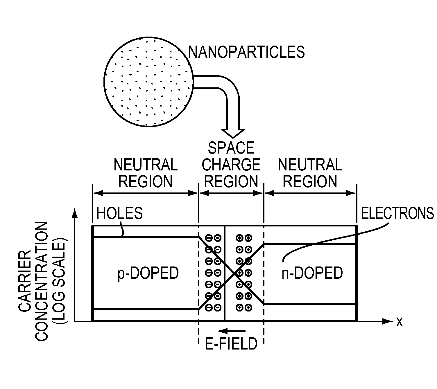
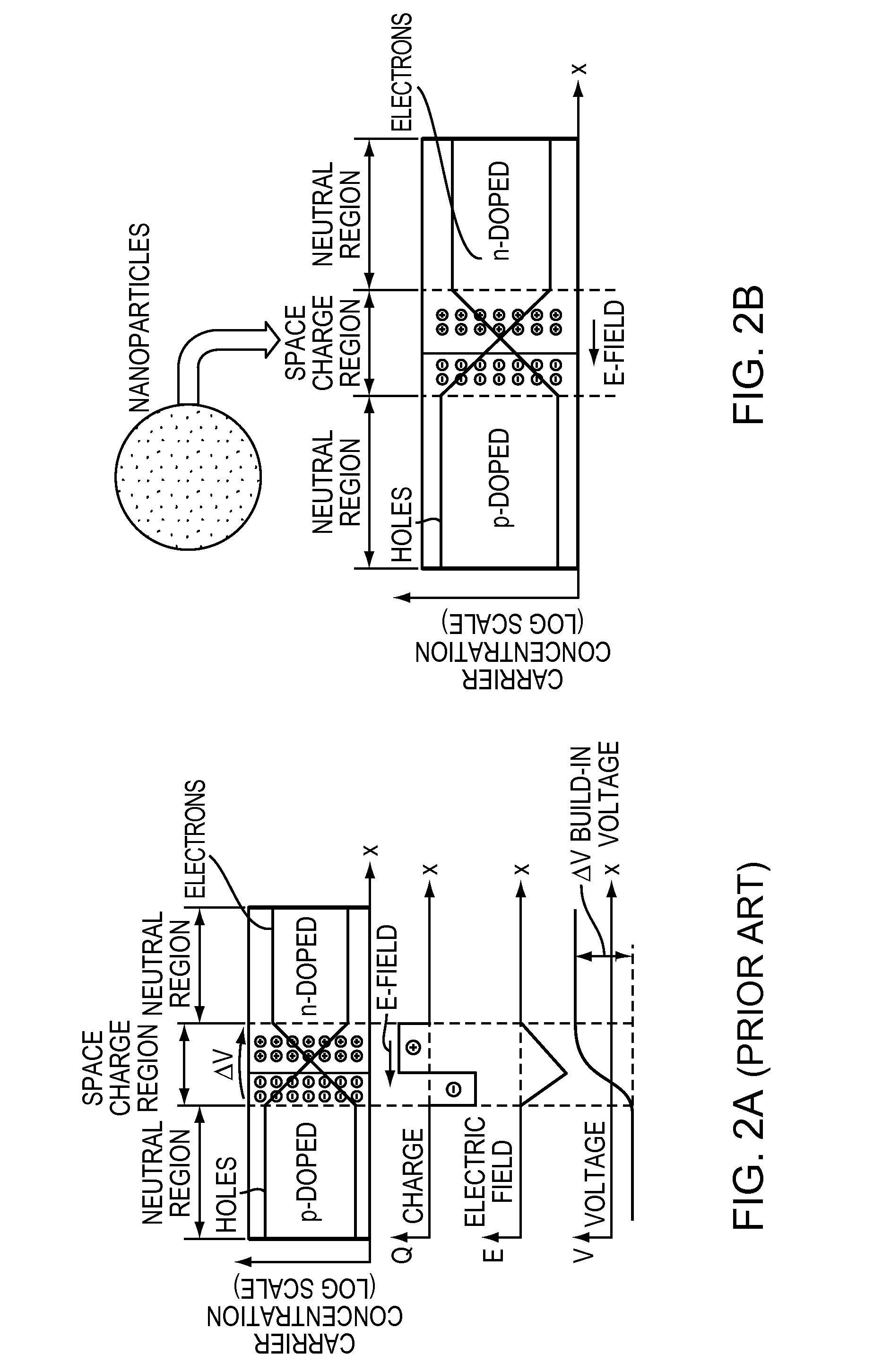
[0050]The break-through concept of semiconductor superlattice heterostructures, first proposed by Esaki and Tsu in the 1970's, can be described as the controlled construction of a nanoscale periodic potential modulation by a designed combination of different materials. Traditional semiconductor or functional oxide superlattices periodically modulate the electronic potential either by composition variation or by a dopant induced electrical field effect.

[0051]Such an artificial layering of multi-phase or doped semiconductors or functional oxides has engineered a variety of functional materials with novel optical and transport properties, leading to a variety of electronic and optoelectronic applications. These electronic and optoelectronic applications may include resonant tunneling devices, lasers, photodiodes, and photodetectors. The thickness of an individual superlattice layer is generally between a few angst...


PUM


Abstract

A method of providing miniaturized size down to nanoscale electronic materials, which may be easily incorporated into the future ever-scaling down power electronics, microelectronics and nanoelectronics device systems, is disclosed. A linear or nonlinear nanoparticle (nanowire) junction design that allows precise controllability over an electronic device (e.g., a varistor) performance, which is typically difficult for the traditional sintered bulk varistor, is also disclosed. A localized doping and chemical modulation, across junctions allows flexible and tunable design over the nanoscale grain boundary band engineering is further disclosed. Furthermore, a method of operating memory, using electrostatic potential modulated coding and decoding across periodic nanoparticle grain boundary linearly, is also disclosed.

Description

RELATED APPLICATION(S)[0001]This application is a divisional of U.S. application Ser. No. 12 / 404,036, filed Mar. 13, 2009, which claims the benefit of U.S. Provisional Application No. 61 / 069,427, filed on Mar. 14, 2008.[0002]The entire teachings of the above application(s) are incorporated herein by reference.BACKGROUND OF THE INVENTION[0003]Currently, bulk polycrystalline varistors are generally used for high voltage circuit protection, while low voltage and ultra-low voltage protection has been a less-touched area without a true analogue product to the high voltage surge arrestor. The general processing methods of prior art varistors typically involve bulk approaches, for example, a polycrystalline sintering process. Such bulk processing does not allow for precise controllability of the various fabrication steps. Furthermore, prior art varistors also lack controllability during operation. Currently, the operating points (e.g., breakdown voltage) of varistors are not capable of bei...

Claims


Application Information

Patent Timeline
IPC IPC(8): H01L29/15H01L21/04
CPCB82Y10/00H01L29/0665H01L29/0673H01L29/0676H01L29/068Y02E10/50H01L31/035227H01L31/03925H01L21/04H01L29/15H01L29/93
Inventor GAO, PU-XIAN
Owner UNIV OF CONNECTICUT
Why Eureka
Try Eureka