Method and apparatus for deposition

a technology of deposition method and deposition apparatus, applied in the direction of chemical vapor deposition coating, solid-state device, final product manufacture, etc., can solve the problems of limiting the application of printed devices, short-circuit and failure of devices, and detrimental to the operation of printed devices obtained, so as to prevent or reduce the diffusion and migration of transferred functional materials

Inactive Publication Date: 2013-07-11
DZP TECH
View PDF3 Cites 18 Cited by
  • Summary
  • Abstract
  • Description
  • Claims
  • Application Information

AI Technical Summary

Benefits of technology

[0050]In a preferred embodiment, there is provided a method and device for pulsed laser deposition by film material transfer where an active material composition is transferred directly, and across a gap, from a media to a receiving substrate under the effect of normally near-infra-red (NIR) but also with some other (e.g. eximer pulsed laser irradiation) to form a printed object which shows functional properties suitable for application in electronic devices. These properties include one or more properties selected from the group consisting of high electronic conductivity, photo-conductivity, light absorption, photovoltaic effects, etc. The deposition process is significantly simplified compared with methods described in the prior art because it does not involve any intermediary coatings and layers, and does not involve significant evaporation and removal of reaction ga...

Problems solved by technology

All of these technologies have certain drawbacks which limit their applications.
This can be detrimental to the operation of the obtained printed device.
For example, it is known that metal atoms from printed metal layers in diodes and transistors easily diffuse and migrate into the adjacent layers, leading to short-circuit and failure of the device.
Additionally, the requirement to use specific solvents in those fluid compositions limit the number and scope of functional materials which can be deposited by trad...

Method used


Image

  • Method and apparatus for deposition
  • Method and apparatus for deposition

Examples


Embodiment Construction

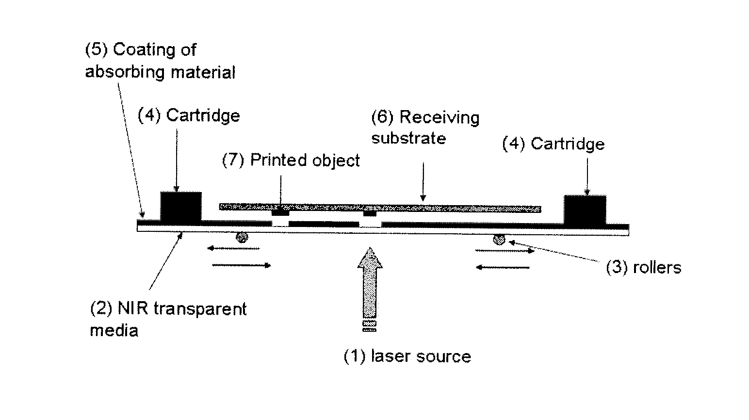
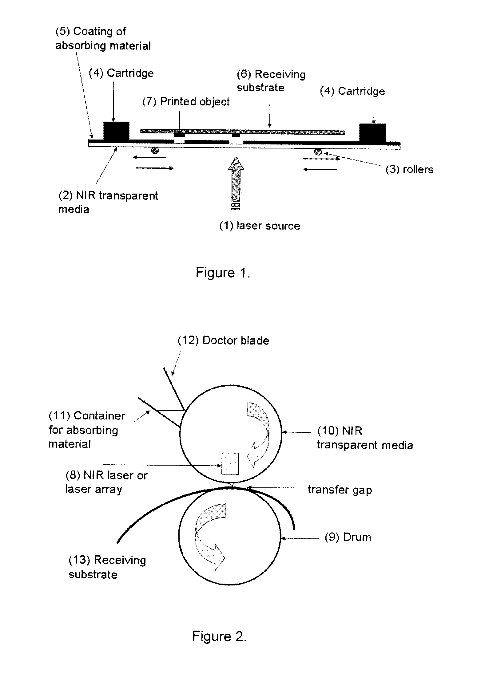
[0077]In the present invention, the laser source consists of a pulsed near-infra-red (NIR—range 800 to 2000 nm) laser or array of lasers. The power density may be optimised according to the beam optics, gap distance, and desired resolution of the printed object. The power density may also be chosen in such a way that the electromagnetic energy is absorbed by the water diluent but is not sufficient to vaporise, decompose or combust the other components of the composition. The power density may be greater than 104 W / cm2. The energy per pulse is preferably up to 5 J / cm2, for example, in the range of 10 micro joules / cm2 to 5 J / cm2. Recently developed laser diodes can achieve shorter pulses in the picosecond and femtosecond range and this makes the transfer system faster and more effective. The exact choice of the beam delivery system may be optimised depending on the required working distances, the focus spot size and absorption properties of the material to be transferred.

[0078]The dev...


PUM

PropertyMeasurementUnit
Temperatureaaaaaaaaaa
Percent by massaaaaaaaaaa

Abstract

The present invention relates to a method of depositing a composition on a receiving substrate to form a printed object, the method comprising the steps of providing: (1) a receiving substrate; (2) a source of near-infra-red laser radiation which is a pulsed laser source or an array of pulsed lasers; (3) a support transparent to near-infra-red laser radiation, the support being positioned between the receiving substrate and the laser source; and a composition which is in contact with the transparent support and which is positioned between the transparent support and the receiving substrate, wherein the composition comprises: (a) a functional material in particulate form capable of absorbing near-infra-red laser radiation, (b) an oligomer and/or polymer, (c) water, and (d) optionally additives, the method comprising directing near-infra-red laser radiation through the transparent support and into the composition and thereby causing the composition to be transferred from the transparent support across a gap to the receiving substrate and causing oligomer and/or polymer to solidify on the receiving substrate, thus forming a printed object on the receiving substrate, wherein the printed object is electrically conductive.
The present invention further provides apparatus, devices, and compositions for use with the method described.

Description

FIELD OF THE INVENTION[0001]The invention is related to a deposition method for the fabrication of a printed object on a flexible or rigid substrate using additive laser assisted non-contact material transfer. The invention is suitable for the printing-like deposition of high precision patterns of useful functionality, for example metallic patterns of high electronic conductivity.DESCRIPTION OF THE RELATED ART[0002]The emerging fields of printed and plastic electronics require the development of new processes and materials which make it possible to fabricate functional prints on flexible substrates such as polymers, papers, textiles and metal foils. Typically, the desired functionality is high electronic conductivity although other functionalities may also be required. Examples include electronic conductivity of controlled levels, dielectric and opto-electronic properties, ionic conductivity, light absorbing properties. These functionalities are useful in the fabrication of differen...

Claims


Application Information

Patent Timeline
IPC IPC(8): H05K3/10
CPCC23C14/06C23C14/28H01L31/022425Y02E10/549H01L31/18H01L51/0013H05K3/10H01L31/0392C23C14/048H01L31/03926Y02P70/50H10K71/18
Inventor TONCHEV, DANZLATKA, STOEVA
Owner DZP TECH
Why Eureka
Try Eureka