Light emitting diode with improved directionality

a light-emitting diode and directionality technology, applied in the direction of semiconductor/solid-state device manufacturing, semiconductor devices, electrical apparatus, etc., can solve the problems of dictating chip performance, light directionality, and major problem of lee for nitride, and achieve the effect of reducing c emission

Inactive Publication Date: 2013-07-25
SHARP KK
View PDF9 Cites 53 Cited by
  • Summary
  • Abstract
  • Description
  • Claims
  • Application Information

AI Technical Summary

Benefits of technology

[0012]A device and method in accordance with the present invention provide a p-side up mounted LED chip with reduced C emission by forming a tapered outwards sidewall structure using a different material to that of the host substrate. This approach does not result in wastage of LED chip area. As used herein, an LED chip is defined as a semiconductor that emits light, including the substrate that the semiconductor is formed on. Further, as used herein a tapered outwards sidewall profile or tapered outwards sidewall structure is defined as a configuration whereby the base area is larger than the area at the top.

Problems solved by technology

However, LEE is a major problem for nitride-based LEDs.
The other issue related to LEE is the light directionality.
Therefore, while an LED chip itself may have good LEE properties, the nature of its high ratio of downward emission would result in package reflectivity ultimately dictating the chip performance.
Reducing sapphire thickness will reduce C emission ratio, but LED chips thinner than 100 μm become difficult to handle in manufacturing environment.
However, this process is more expensive and complicated over conventional p-side up mounting.
However, there are high costs associated with producing LED package with very high reflectivity.
Manufacturing a tapered outwards structure will result in a significant loss of active area, since the active region on the tapered sapphire areas is wasted (refer to FIG. 6A).
As a result, it may not be economically viable to manufacture such a structure.
P-side down mounting process is however more complex in manufacturing environment over p-side up structures.
High index films / resin / epoxy is more effective for light extraction, but is also more expensive than low index films.

Method used


Image

  • Light emitting diode with improved directionality
  • Light emitting diode with improved directionality
  • Light emitting diode with improved directionality

Examples


embodiment 1

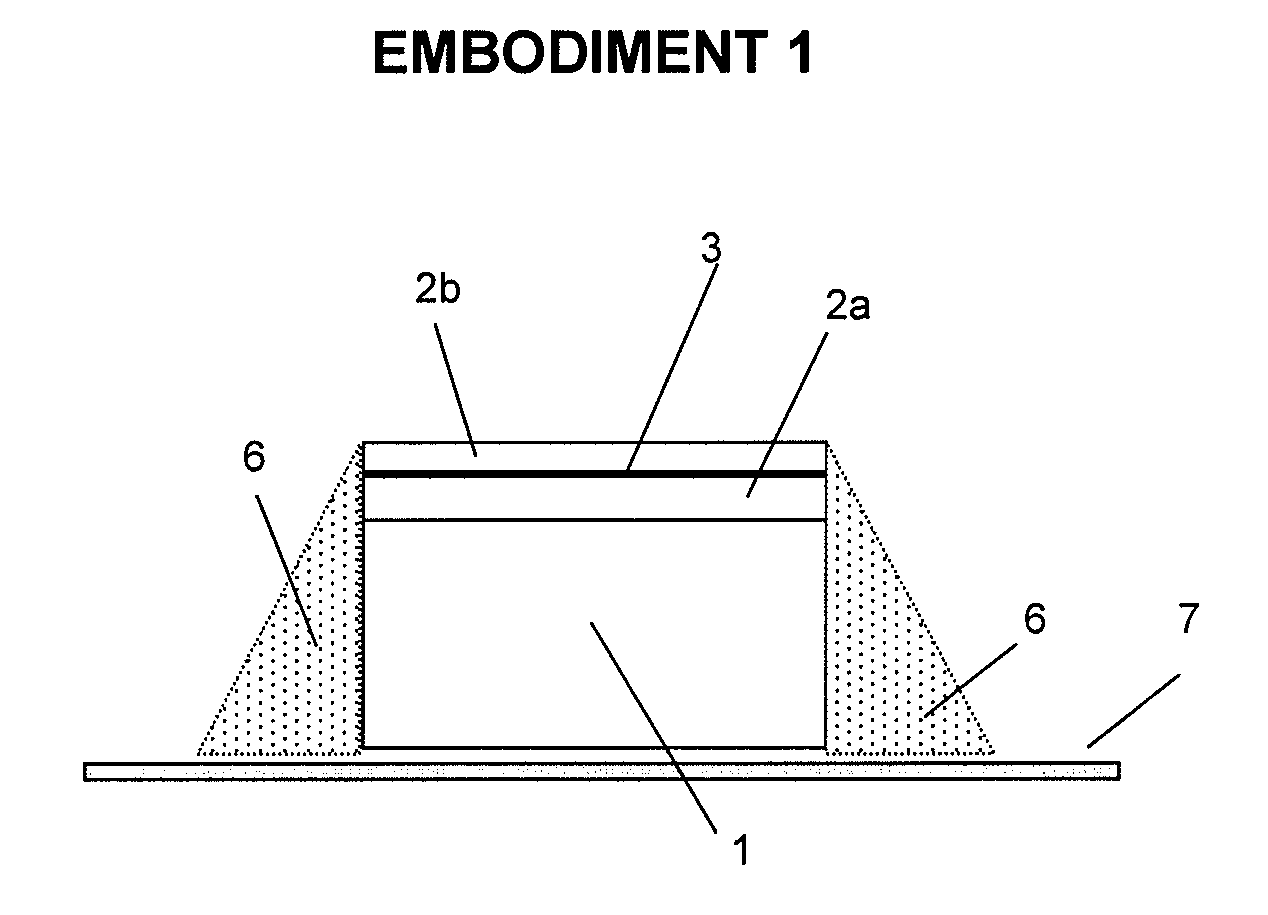
[0065]FIG. 7 illustrates an exemplary device structure in accordance with first embodiment (Embodiment 1) of the invention. The tapered outwards portion of the structure 6 is made from the different material (a second material) to that of the host substrate (a first material). The tip of the tapered outwards region can be higher, lower or similar to the LED chip. The reflector base of the LED package 7 is an imaginary layer where the LED is typically mounted. The refractive index of the tapered outwards portion 6 is ideally similar to the host substrate (refractive index of sapphire is ˜1.77@450 nm). Examples of transparent material in this refractive index range that can be used include SiOxNy, Optindex D54, Norland adhesives or other materials. However, this material can also be of lower refractive index than the host material. It is important to note that the inventive approach has a significantly different concept to the prior art structure described in FIG. 5A. The method of en...

embodiment 2

[0067]FIG. 9 is an illustration of a second embodiment (Embodiment 2) in accordance with the invention. For this structure, the tapered outwards structure is made from a series of material with different refractive indices. As example, layer 10 will have a similar or lower refractive index than the host substrate 1, and layer 11a lower refractive index than layer 10, and layer 12 being lower than layer 11. Any number of layers for the tapered outwards portion can be used in this structure, with any combination of refractive indices. It is not necessary for the refractive index to be graded or to follow a particular trend. In theory, by grading the refractive index from high to low moving outwards of the structure can improve LEE.

embodiment 3

[0068]FIG. 10 is an illustration of a third embodiment (Embodiment 3) in accordance with the invention. For this structure, the tapered outwards structure is formed externally on the LED package or reflector side, the LED package including a base formed from a first material and the tapered structure formed from a second material. This approach has the added advantage of not having to shape the LED sidewalls, therefore simplifying the manufacturing process. Instead of forming the tapered outwards portion on the LED chip, the tapered outwards structure 13 is pre-formed on the LED module package base 14, for example as pocket columns (e.g., preformed sidewalls into which the LED package may be inserted). In the case of a high power LED module, a series of pockets are then formed on the package base. It is not essential for the height of the pocket structure to be similar to that of the LED chip. The tapered sidewall 13 is ideally transparent and can be made of the same or different ma...


PUM


Abstract

A light emitting diode (LED) is provided that includes a host substrate formed from a first material, an n-type layer formed over the host substrate, an active region formed over the n-type layer, and a p-type layer formed over the active region. A layer is formed adjacent to the host substrate and includes a second material, the second material being different from the first material or having a refractive index different from a refractive index of the first material. Further, the second material is formed with a tapered outwards sidewall profile.

Description

TECHNICAL FIELD OF THE INVENTION[0001]The present invention relates to a light emitting diode (LED) device and a method of making the same, and in particular an LED device structure with tapered outwards sidewalls, with the tapered portion made of a different material to that of the LED host substrate.BACKGROUND OF THE INVENTION[0002]In recent years, the use of light emitting diodes (LED) as a light source to replace incandescent bulbs and compact fluorescent lamps (CFL) for general lighting and backlight applications is becoming increasingly popular. LEDs have the advantage of higher efficiency over conventional light sources and the use of non-toxic materials. Research laboratories have reported LEDs with efficacies of 200 lm / W, while commercially available chips are currently yielding ˜100 lm / W. Theoretically, the maximum efficacy of an LED chip is between 300-400 lm / W, thus there is still plenty of room for further improvement.[0003]An indium gallium nitride-based (InGaN) blue L...

Claims


Application Information

Patent Timeline
Patent Type & Authority Applications(United States)
IPC IPC(8): H01L33/58H01L33/48
CPCH01L2933/005H01L33/54
Inventor TAN, WEISINBROCKLEY, MICHAEL JOHNBERRYMAN-BOUSQUET, VALERIE
Owner SHARP KK
Why Eureka
Try Eureka