Semiconductor device and method for manufacturing the same

a semiconductor device and semiconductor technology, applied in semiconductor devices, diodes, electrical devices, etc., can solve the problems affecting the time and cost of a semiconductor device manufacture, and achieve the effects of reducing the resistance between the source electrode and the drain electrode of the transistor, improving the electric characteristics of the semiconductor device, and efficient formation

Active Publication Date: 2013-08-01
SEMICON ENERGY LAB CO LTD
View PDF3 Cites 41 Cited by
  • Summary
  • Abstract
  • Description
  • Claims
  • Application Information

AI Technical Summary

Benefits of technology

[0021]By manufacturing the semiconductor device by the above method, the transistor and the capacitor can be formed through the same process; therefore, the capacitor can be efficiently formed. Further, since the second electrode film is connected onto the oxide semiconductor film between the first electrode film and the channel formation region of the transistor. Resistance between the source electrode and the drain electrode of the transistor can be reduced; accordingly, electric characteristics of the semiconductor device can be improved.
[0022]Note that in the above-described method for manufacturing the semiconductor device, a second element formation layer including a transistor formed using silicon, germanium, or a compound semiconductor material for its active layer is formed, the first element formation layer is formed over the second element formation layer, and the transistor included in the second element formation layer is electrically connected at least to the transistor or the capacitor included in the first element formation layer, whereby the semiconductor device with higher speed operation and low power consumption can be achieved.
[0023]Further, in the above-described method for manufacturing the semiconductor device, the active layer of the transistor included in the second element formation layer can be formed using a film obtained by separation of part of a single crystal semiconductor substrate or a compound semiconductor substrate, whereby the thickness of the transistor can be thin. Accordingly, the transistor can be made a partial depleted or fully depleted transistor; accordingly, the semiconductor device with high speed operation and low power consumption can be achieved.
[0024]Note that the first element formation layer and the second element formation layer over the first element formation layer can be formed over a flexible substrate, whereby the semiconductor device can have added values such that the semiconductor device can be mounted even on a curved surface or an uneven surface, the device is less likely to be damaged even when dropped, or the device is light in weight.
[0025]A source electrode and a drain electrode of a transistor has a two-layer structure, and a capacitor is formed using a first electrode film, a gate insulating film, and a gate electrode of the transistor. Accordingly, the transistor and the capacitor can be formed through the same process; therefore, the capacitor can be efficiently formed.
[0026]Further, a second electrode film is connected onto an oxide semiconductor film between the first electrode film and a channel formation region of the transistor. Accordingly, resistance between the source electrode and the drain electrode can be reduced; therefore, electric characteristics of the semiconductor device can be improved.

Problems solved by technology

Further, how efficiently capacitors provided in various portions in a semiconductor device are formed influences time and cost for a manufacture of the semiconductor device.

Method used


Image

  • Semiconductor device and method for manufacturing the same
  • Semiconductor device and method for manufacturing the same
  • Semiconductor device and method for manufacturing the same

Examples


embodiment 1

[0058]In this embodiment, an example of a structure of a semiconductor device and a method for manufacturing the semiconductor device will be described with reference to FIGS. 1A to 1D, FIGS. 2A to 2C-2, FIGS. 3A to 3D, FIGS. 4A to 4D, FIG. 5, FIGS. 6A to 6C, and FIG. 7.

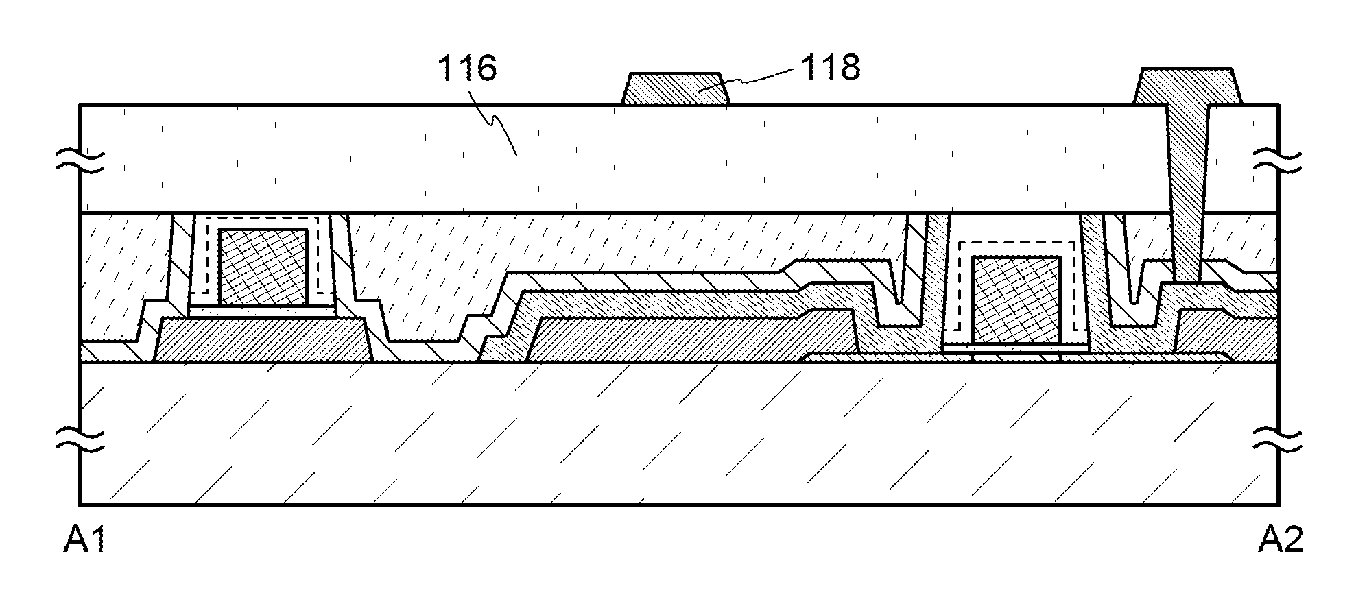
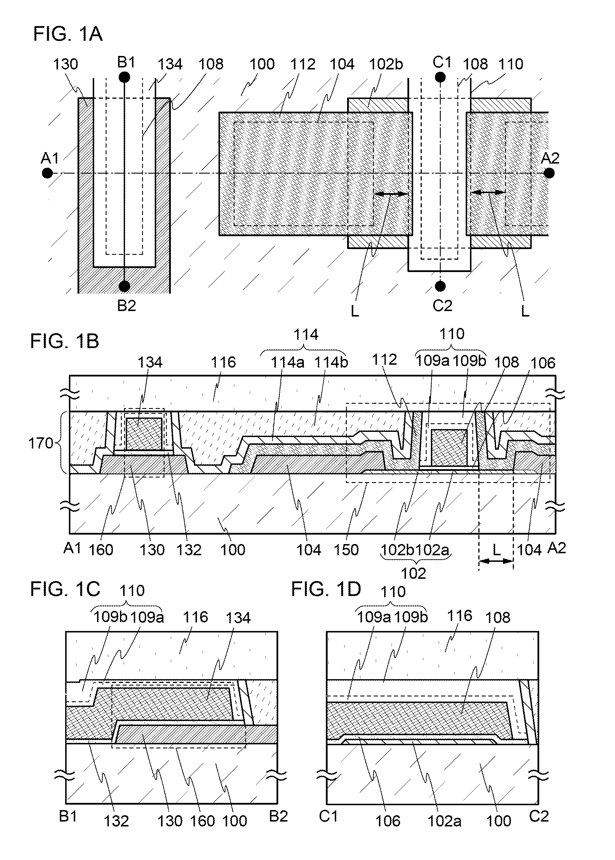
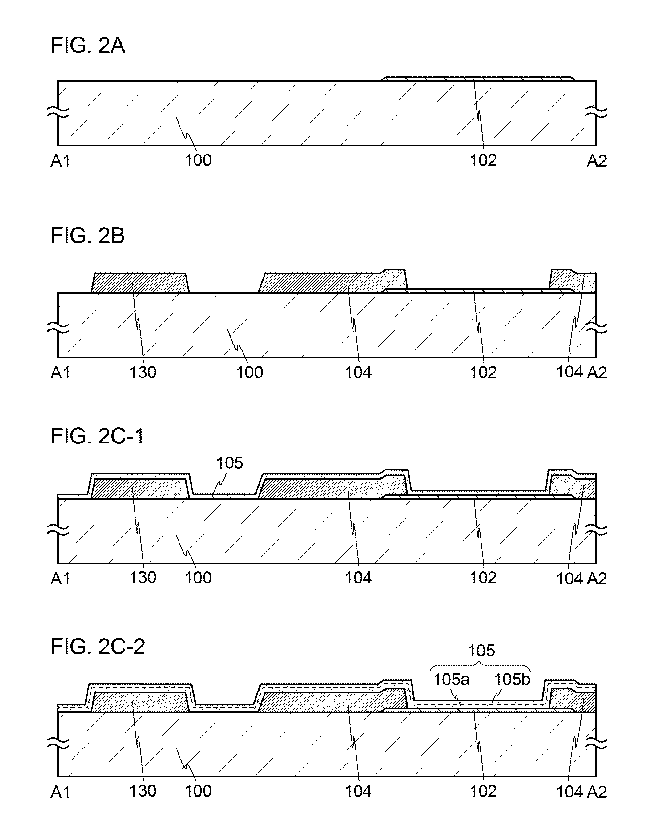
[0059]FIGS. 1A to 1D show an example of a plan view and cross-sectional views of a semiconductor device including an element formation layer 170 including a top-gate transistor 150 and a capacitor 160. FIG. 1A is a plan view, FIG. 1B is a cross-sectional view taken along a dashed-dotted line A1-A2 in FIG. 1A, FIG. 1C is a cross-sectional view taken along a dashed-dotted line B1-B2 in FIG. 1A, and FIG. 1D is a cross-sectional view taken along a dashed-dotted line C1-C2 in FIG. 1A.

[0060]The element formation layer 170 in FIGS. 1A to 1D includes the transistor 150 and the capacitor 160. The transistor 150 has a structure which includes: an oxide semiconductor film 102 provided over a substrate 100 having an insulating s...

embodiment 2

[0181]In this embodiment, one embodiment of a structure and a manufacturing method of a semiconductor device whose structure is different from that described in Embodiment 1 will be described with reference to FIGS. 8A to 8D and FIGS. 9A to 9D.

[0182]FIGS. 8A to 8D show an example of a plan view and cross-sectional views of a semiconductor device including an element formation layer 870 including a top-gate transistor 850 and a capacitor 860. FIG. 8A is a plan view, FIG. 8B is a cross-sectional view taken along a dashed-dotted line F1-F2 in FIG. 8A, FIG. 8C is a cross-sectional view taken along a dashed-dotted line G1-G2 in FIG. 8A, and FIG. 8D is a cross-sectional view taken along a dashed-dotted line H1-H2 in FIG. 8A. In FIG. 8A, part of components is omitted to avoid complexity of the drawing.

[0183]The element formation layer 870 in FIGS. 8A to 8D includes the transistor 850 and the capacitor 860. The transistor 850 has a structure which includes: an oxide semiconductor film 102 p...

embodiment 3

[0197]In this embodiment, one embodiment of a structure and a manufacturing method of a semiconductor device whose structure is different from that described in the above-described embodiments will be described with reference to FIGS. 10A to 10D and FIGS. 11A to 11D.

[0198]FIGS. 10A to 10D show an example of a plan view and cross-sectional views of a semiconductor device including an element formation layer 1070 including a top-gate transistor 1050 and a capacitor 1060. FIG. 10A is a plan view, FIG. 10B is a cross-sectional view taken along a dashed-dotted line I1-I2 in FIG. 10A, FIG. 10C is a cross-sectional view taken along a dashed-dotted line J1-J2 in FIG. 10A, and FIG. 10D is a cross-sectional view taken along a dashed-dotted line K1-K2 in FIG. 10A. In FIG. 10A, part of components is omitted to avoid complexity of the drawing.

[0199]The element formation layer 1070 in FIGS. 10A to 10D includes the transistor 1050 and the capacitor 1060. The transistor 1050 has a structure which i...


PUM


Abstract

A semiconductor device having high electric characteristics and in which a capacitor is efficiently formed even if the semiconductor device has a miniaturized structure. In a top-gate (also referred to as staggered) transistor using an oxide semiconductor film as its active layer, a source electrode and a drain electrode has a two-layer structure (a first electrode film and a second electrode film). Then, a capacitor is formed using a film formed using a material and a step similar to those of the first electrode film, a gate insulating film, and a gate electrode. Accordingly, the transistor and the capacitor can be formed through the same process efficiently. Further, the second electrode is connected onto the oxide semiconductor film between a first electrode and a channel formation region of the transistor. Accordingly, resistance between source and drain electrodes can be reduced; therefore, electric characteristics of the semiconductor device can be improved.

Description

BACKGROUND OF THE INVENTION[0001]1. Field of the Invention[0002]The present invention relates to a semiconductor device and a method for manufacturing the semiconductor device.[0003]In this specification, a semiconductor device generally means a device which can function by utilizing semiconductor characteristics, and an electro-optic device, a semiconductor circuit, and electronic equipment are all semiconductor devices.[0004]2. Description of the Related Art[0005]Transistors in which an active layer is formed using a semiconductor thin film which is formed over a substrate having an insulating surface are widely used in electronic devices such as integrated circuits (ICs) and image display devices (display devices). A silicon-based semiconductor material is widely known as a material for a semiconductor thin film applicable to a transistor. As another material, an oxide semiconductor has been attracting attention.[0006]For example, a transistor whose active layer includes an amorp...

Claims


Application Information

Patent Timeline
Patent Type & Authority Applications(United States)
IPC IPC(8): H01L27/06H01L29/66
CPCH01L27/0629H01L29/66969H01L27/1156H01L27/1255H01L27/1225H10B41/70H01L27/1222H01L27/1259H01L29/78651H01L29/78681H01L29/78684H01L29/7869
Inventor YAMAZAKI, SHUNPEI
Owner SEMICON ENERGY LAB CO LTD
Why Eureka
Try Eureka