Coating Method for an Optoelectronic Chip-on-Board Module

a chip-on-board module and optoelectronic technology, applied in the direction of printed circuit dielectrics, transparent dielectrics, printed circuit aspects, etc., can solve the problems of coating negatively affecting the light emission intensity or light sensitivity of optoelectronic chip-on-board modules, and high modularity. , the effect of simple and cost-efficient production sequen

Inactive Publication Date: 2013-08-01
HERAEUS NOBLELIGHT GMBH
View PDF6 Cites 37 Cited by
  • Summary
  • Abstract
  • Description
  • Claims
  • Application Information

AI Technical Summary

Benefits of technology

[0117]Another advantage of the present invention consists in the possibility of a realization of high modularity. Thus, for example, optoelectronic chip-on-board modules can each be realized having one or more one-dimensional or two-dimensional arrays of optoelectronic components, wherein these arrays can have identical constructions. Several such optoelectronic chip-on-board modules, especially having identical arrays of optoelectronic components, can be connected in series to each other in one or two spatial directions. The identity of the arrays of optoelectronic components, for example the LED arrays, can be advantageous for a simple and cost-efficient production sequence. Overall, advantages with regard to an adaptation to different processing geometries can be realized in this way.
[0118]These individual advantages that can be realized according to the invention or also combinations of these advantages can cause a direct increase in the efficiency of the optoelectronic chip-on-board module and / or the system, for example the emitter. In this way, for example, very high irradiation strengths can be achieved for simultaneously homogeneous irradiation strength distributions, even with large distances. The listed advantages can also be combined with each other in pairs or in groups arbitrarily. The spectrum of possibilities that can be realized is therefore high, wherein a plurality of requirements can be fulfilled.

Problems solved by technology

Protection in the form of housings on chip-on-board modules is often expensive and technologically complicated.
The plastic dam generated in this way, however, is not transparent.
Therefore, this method of coating negatively affects the light emission intensity or light sensitivity of optoelectronic chip-on-board modules, that is, chip-on-board modules populated at their edges with optoelectronic components, for example LEDs or photodiodes.
These mentioned methods using epoxy resins are less suitable for optoelectronic use, because epoxy resins are not UV-resistant and temperature-resistant.
Thus, they are not stable, for example, in a high-power UV-LED module or also under intense sunlight irradiation having UV components, as can occur in photovoltaic systems.
They age quickly under UV exposure and are destroyed.
Other transparent, UV-resistant, and temperature-resistant solutions, for example bonding a glass frame or a glass cup, require a very complicated assembly of the frame and a compactness of the frame that can be produced only with difficulty.
For rigid glass materials, a usually necessary adaptation of the thermal expansion coefficients of the compound materials also represents another hurdle, especially if the resulting products are exposed to thermal cycles.
In a combination solution made of a glass frame and an encapsulation with a suitable non-epoxy-based material, e.g., a temperature-resistant and UV-resistant silicone, very small gaps between the frame and substrate can have the result that the silicone, which is strongly susceptible to creep, can run out during the casting.
This negatively affects a best possible utilization of the substrate surface area and / or a desired stackability.
This results in a loss of usable surface area on the module, because the edge area must be kept free from components.
Up until now, no method for realizing a flat coating for chip-on-board modules has been known in which materials can be used both in the face area and also in the edge area of the casting, which materials are both UV-resistant and also temperature-resistant and that are also transparent for electromagnetic radiation from the ultraviolet to the infrared spectral range.
With this method it is not possible to provide optoelectronic chip-on-board modules with a coating that is transparent, UV-resistant, and temperature-resistant and that can be populated arbitrarily with optoelectronic components, especially while utilizing the entire surface area.

Method used


Image

  • Coating Method for an Optoelectronic Chip-on-Board Module
  • Coating Method for an Optoelectronic Chip-on-Board Module
  • Coating Method for an Optoelectronic Chip-on-Board Module

Examples


Embodiment Construction

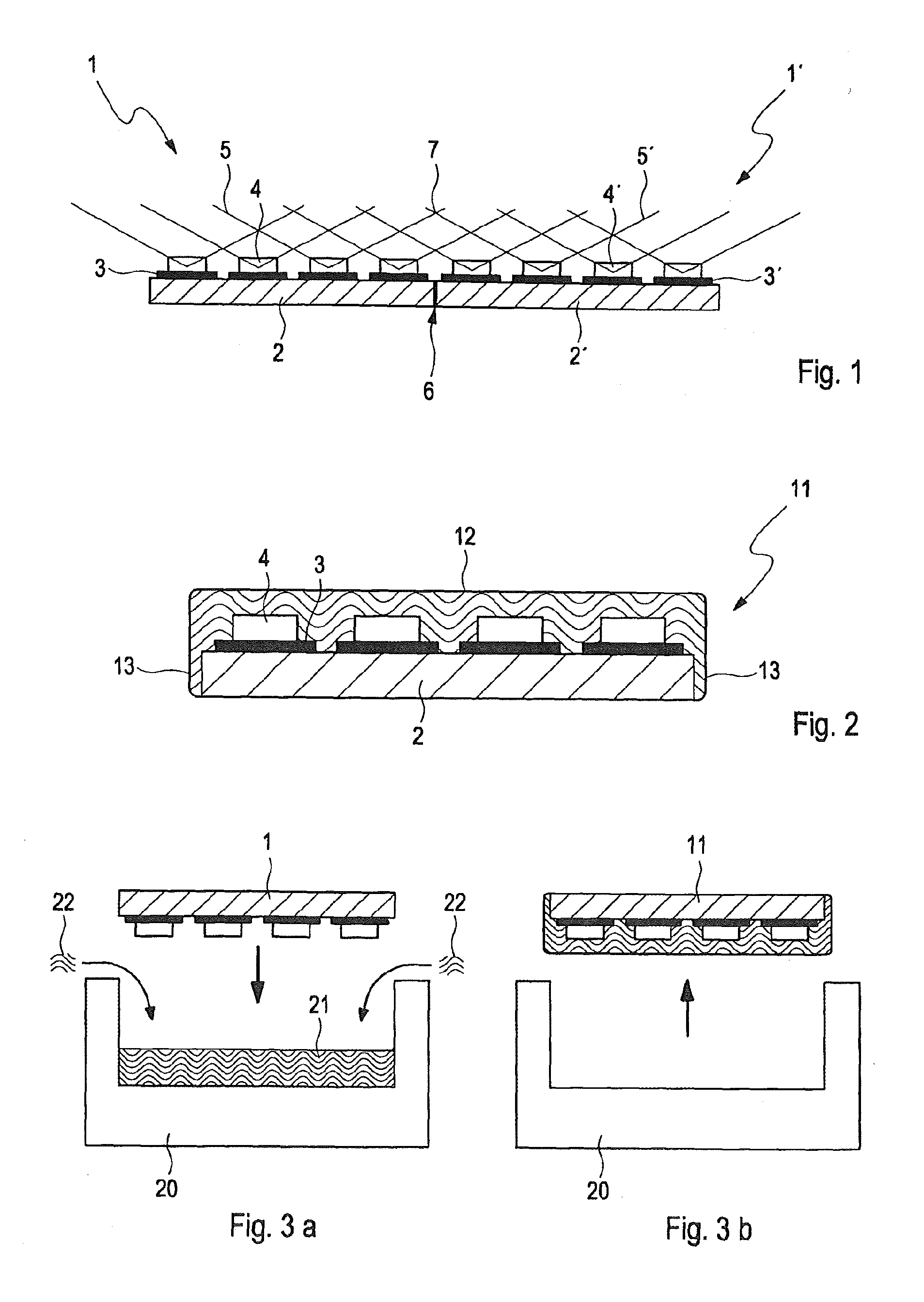
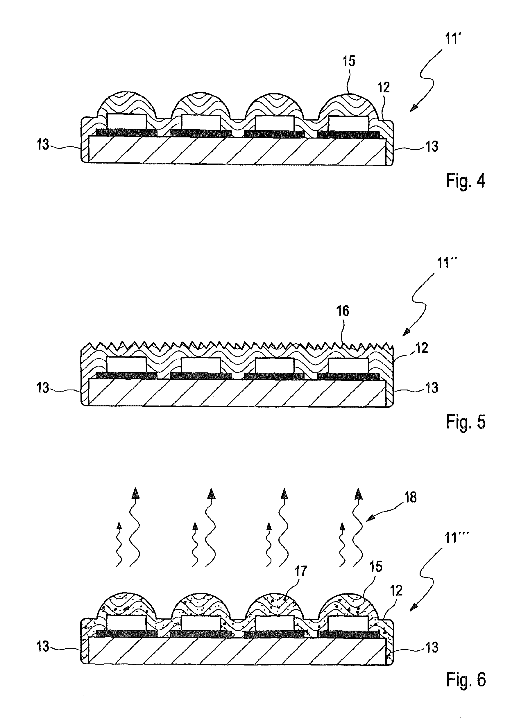
[0136]The invention is explained with reference to chip-on-board LED modules, that is light-emitting bodies, as an example for optoelectronic chip-on-board modules. Within the scope of the invention photodiodes in solar cells or other components could be used as the optoelectronic components instead of LED modules.

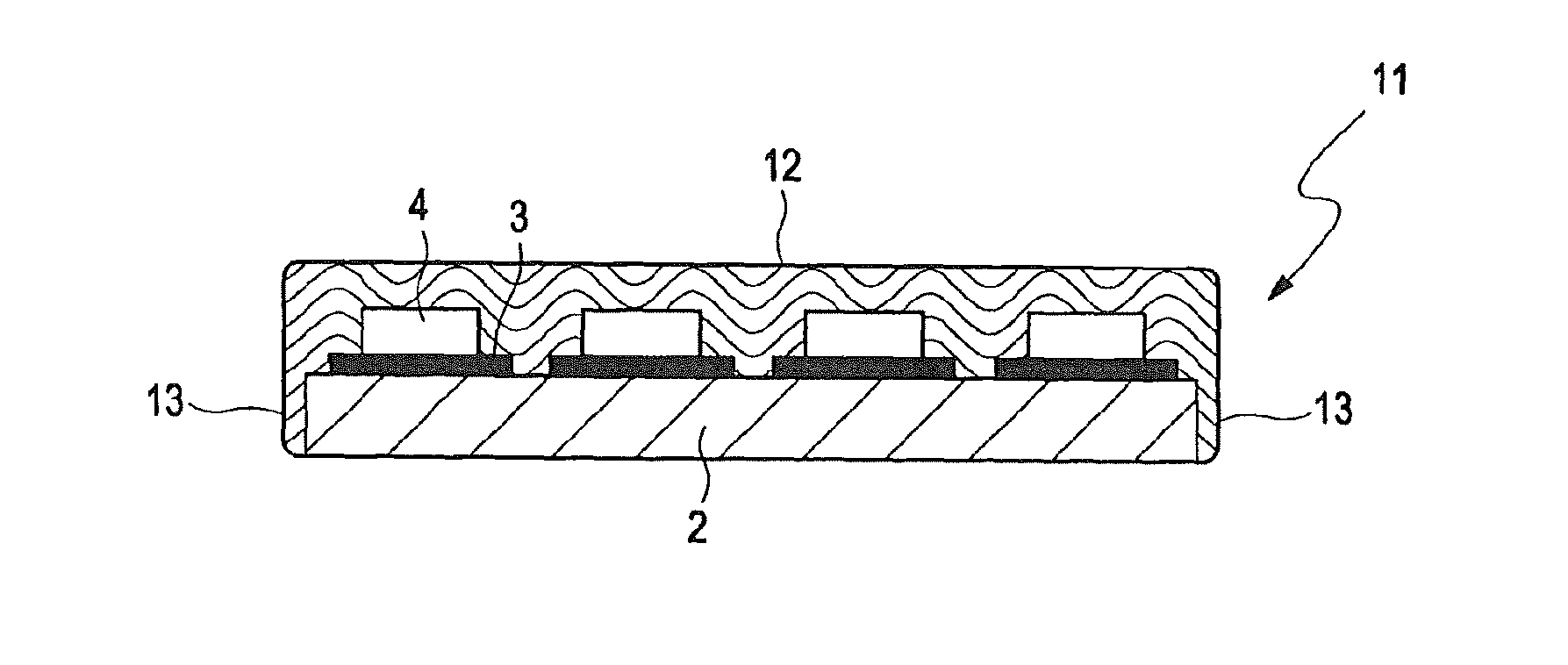
[0137]FIG. 1 shows schematically in cross section a chip-on-board LED module 1 without coating, in which strip conductors 3, 3′ and LEDs 4, 4′ formed as non-housed LED chips are arranged in regular spacing on two parallel substrates 2, 2′ or carriers. For reasons of clarity, not all recurring elements of FIG. 1 and the following figures are provided with reference symbols, but these all refer to identical elements. Thus, in FIG. 1 only one LED 4, 4′ is designated for each of the two chip-on-board LED modules 1, 1′ with a reference symbol. The other components are identical.

[0138]A substrate 2, 2′ can be, for example, a metal, ceramic, or silicon substrate built using rigid...


PUM

PropertyMeasurementUnit
atmospheric pressureaaaaaaaaaa
pressureaaaaaaaaaa

Abstract

A method is proposed for coating an optoelectronic chip-on-board module including a flat substrate populated with one or more optoelectronic components having at least one primary optical arrangement and optionally at least one secondary optical arrangement. The optoelectronic chip-on-board module is coated with a transparent, UV-resistant, and temperature-resistant coating made of silicone by the following steps: (a) casting a liquid silicone into a mold open towards the top and having outer dimensions corresponding to or exceeding outer dimensions of the substrate; (b) inserting the substrate into the mold, wherein the optoelectronic component(s) are immersed completely into the silicone and a surface of the substrate contacts the silicone completely or the substrate immerses into the silicone at least partially with full surface contact; (c) curing and cross-linking the silicone with the optoelectronic component(s) and the substrate; and (d) removing the substrate from the mold with the coating of cured silicone.

Description

CROSS-REFERENCE TO RELATED APPLICATIONS[0001]This application is a Section 371 International Application No. PCT / EP2011 / 004326, filed Aug. 29, 2011, which was published in the German language on Mar. 15, 2012, under International Publication No. WO 2012 / 031703 A1 and the disclosure of which is incorporated herein by reference.BACKGROUND OF THE INVENTION[0002]The invention relates to a method for coating an optoelectronic chip-on-board module, comprising a flat substrate populated with one or more optoelectronic components, with a transparent, UV-resistant, and temperature-resistant coating made of a silicone, a corresponding optoelectronic chip-on-board module, and a system having multiple optoelectronic chip-on-board modules.[0003]Generic optoelectronic chip-on-board modules are used, for example, as illuminating bodies, as high-power UV LED lamps, as photovoltaic modules, as sensors, or as similar devices. Within the scope of the invention optoelectronic components used in this wa...

Claims


Application Information

Patent Timeline
Patent Type & Authority Applications(United States)
IPC IPC(8): H01L33/54H01L31/0203
CPCF21K9/00H01L33/58F21Y2101/02H01L21/56H01L23/3121H01L25/0753H01L33/54H01L33/60H01L2933/005H05K3/284H05K2201/0108H05K2201/0162H05K2201/10106H05K2201/10121H05K2201/10151H05K2203/1316H01L31/0203H01L2924/1815H01L2924/0002F21K9/90H01L33/56H01L25/13H01L31/02322H01L31/02325H01L33/507H01L2924/00F21Y2115/10B29D11/00298H01L23/31H05K3/28B29C41/00H01L27/00
Inventor PEIL, MICHAELOSWALD, FLORINMAIWEG, HARALD
Owner HERAEUS NOBLELIGHT GMBH
Why Eureka
Try Eureka