Silicon etchant and method for producing transistor by using same

a technology of silicon etchant and etchant, which is applied in the direction of electrical equipment, semiconductor devices, chemistry apparatus and processes, etc., can solve the problems of large power consumption, increased leakage current owing to tunnel current, excessively small oxidation, etc., and achieves selective removal of silicon, high quality, and high precision

Inactive Publication Date: 2013-08-08
MITSUBISHI GAS CHEM CO INC
View PDF4 Cites 9 Cited by
  • Summary
  • Abstract
  • Description
  • Claims
  • Application Information

AI Technical Summary

Benefits of technology

[0027]According to the present invention, in a process for producing a transistor including a laminate formed of at least a high dielectric material film and an aluminum metal gate by the method in which a dummy gate made of silicon is removed and replaced with the aluminum metal gate, it is possible to selectively remove the silicon by etching. As a result, according to the present invention, it is possible to produce a transistor having a high precision and a high quality with a high yield.
[0028]The silicon etching solution according to the present invention is used for etching a dummy gate made of silicon in a process for producing a transistor using a structural body which includes a substrate, and a dummy gate laminate formed by laminating at least a high dielectric material film and the dummy gate made of silicon, a side wall disposed to cover a side surface of the laminate and an interlayer insulating film disposed to cover the side wall which are provided on the substrate, such that the dummy gate is replaced with an aluminum metal gate. The silicon etching solution includes 0.1 to 40% by weight of at least one alkali compound selected from the group consisting of ammonia, a diamine and a polyamine represented by the following general formula (1), 5 to 50% by weight of at least one polyhydric alcohol represented by the following general formula (2) and 40 to 94.9% by weight of water,
[0029]The alkali compound used in the present invention serves for etching silicon, and is at least one compound selected from the group consisting of ammonia, a diamine and a polyamine represented by the general formula (1). Examples of the preferred diamine contained in the silicon etching solution according to the present invention include ethylenediamine, 1,2-propanediamine and 1,3-propanediamine. Examples of the preferred polyamine represented by the general formula (1) include diethylenetriamine and triethylenetetramine.
[0030]The concentration of the alkali compound in the etching solution is usually from 0.1 to 40% by weight, preferably from 0.2 to 40% by weight and more preferably from 0.3 to 30% by weight.
[0031]The polyhydric alcohol contained in the silicon etching solution according to the present invention is at least one compound selected from the group consisting of those compounds represented by the general formula (2). Specific examples of the preferred polyhydric alcohol represented by the general formula (2) include glycerin, meso-erythritol, xylitol and sorbitol.
[0032]The concentration of the polyhydric alcohol in the etching solution is usually from 5 to 50% by weight, preferably from 6 to 40% by weight and more preferably from 7 to 30% by weight. When the concentration of the polyhydric alcohol in the etching solution is 5% by weight or more, the resulting etching solution can exhibit a sufficient effect of preventing corrosion of aluminum. On the other hand, when the concentration of the polyhydric alcohol in the etching solution is 50% by weight or less, the resulting etching solution can exhibit a sufficient silicon etching capability.

Problems solved by technology

However, if it is intended to achieve the micronization of transistors as recently required, a gate thickness of a conventional gate insulating film using silicon oxide becomes excessively small, so that a leakage current owing to a tunnel current increases, and power consumption becomes large.
If such a protective film is formed, the production process tends to become complicated, so that there tend to arise the problems such as poor yield and increase in production costs.
In addition, an asking treatment required to remove the photoresist tends to cause damage to the aluminum and interlayer insulating film, which tends to cause a risk of deteriorating a performance of transistors.
In the dry-etching process, a high dielectric material exposed after etching the silicon tends to be etched or tends to be deteriorated in quality when subjected to the overetching, resulting in deterioration in performance of transistors.
Therefore, when the above technique is carried out using a sheet cleaning apparatus for cleaning a silicon wafer one by one which has been recently used usually in production of semiconductors to suppress generation of particles in a wet etching method, it is not possible to attain a stable etching capability.
If the etching is conducted at a temperature at which the sheet cleaning apparatus is usable, the etch rate of silicon tends to be excessively low.
Thus, the above technique is not applicable to etching of silicon in a step of forming a transistor including a high dielectric material and a metal gate.
For this reason, the technique is not applicable to a step of forming a transistor portion of semiconductors in which even fine particle residues are not allowed to remain.
In addition, the technique is unsatisfactory to be used in a step of forming a transistor in a semiconductor in which etching of even a slight amount of aluminum should not be allowed (refer to Comparative Example 2).
However, in this technique, since an etch rate of aluminum is excessively high, the technique is not applicable to etching of silicon in a step of forming a transistor including a high dielectric material and a metal gate (refer to Comparative Example 3).
However, the technique described in Patent Document 4 relates to the method of preventing etching of aluminum from the viewpoint of removal of chlorine, and therefore fails to specify a silicon etching capability of the alkaline stripping solution.
Thus, Patent Document 5 fails to describe a silicon etching capability of the alkaline stripping solution.
However, alkaline compounds capable of etching silicon are limited to specific compounds.
However, the cleaning solution has a low silicon etching capability and therefore is unsuitable for achieving the object as aimed by the present invention (refer to Comparative Examples 6).

Method used


Image

  • Silicon etchant and method for producing transistor by using same
  • Silicon etchant and method for producing transistor by using same

Examples


examples

[0056]The present invention will be described in more detail below by referring to the following examples. It should be noted, however, that the following examples are only illustrative and not intended to limit the invention thereto.

Evaluation Method

Measuring Equipments:

[0057]Fluorescent X-ray analysis: Measured using “SEA1200VX” available from SII Nano Technology Inc.

[0058]SEM observation: Observed using an ultrahigh resolution field emission type scanning electron microscope “S-5500” available from Hitachi Hi-Technologies Corp.

[0059]FIB Fabrication: Fabricated using a focused ion beam fabrication device “FB-2100” available from Hitachi Hi-Technologies Corp.

[0060]STEM Observation: Observed using a scanning transmission electron microscope “HD-2300” available from Hitachi Hi-Technologies Corp.

Determination:

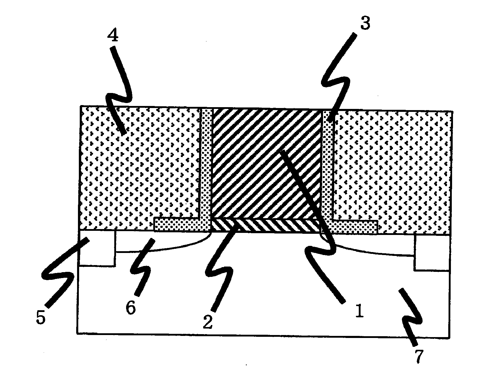
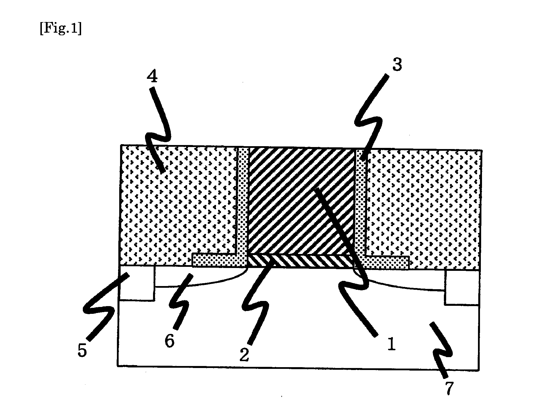
(Etching Condition of Dummy Gate 1 Made of Silicon)

[0061]◯: Dummy Gate 1 was completely etched.

[0062]X: Dummy Gate 1 was insufficiently etched.

(Evaluation of Corrosion Resistance...

examples 1 to 48

[0065]In order to examine a corrosion resistance of the etching solution to aluminum, the following procedure was used. That is, a 1000 Å-thick aluminum film was deposited on a silicon wafer as a substrate by PVD. The aluminum film thus deposited on the substrate was immersed in the etching solution shown in Table 2 at 25° C. for 30 min, and the thickness of the aluminum film before and after the immersion was measured by a fluorescent X-ray analyzer to calculate an amount of the aluminum film etched with the etching solution. Further, an etch rate of aluminum was calculated from the amount of the aluminum film etched and the immersion time. When the etch rate of aluminum is less than 1 nm / min, it was determined that the etching solution had a corrosion resistance to aluminum.

[0066]Next, testing methods for a silicon etching capability of the etching solution and a corrosion resistance thereof to the high dielectric material film, side wall and interlayer insulating film are explain...


PUM

PropertyMeasurementUnit
dielectricaaaaaaaaaa
weightaaaaaaaaaa
lengthaaaaaaaaaa

Abstract

According to the present invention, there is provided an etching solution used for selectively etching a dummy gate made of silicon in a process for producing a transistor including a laminate formed of at least a high dielectric material film and an aluminum metal gate by the method of removing the dummy gate made of silicon to replace the dummy gate with the aluminum metal gate, and a process for producing a transistor using the etching solution. The present invention relates to a silicon etching solution used for etching the dummy gate made of silicon which includes 0.1 to 40% by weight of at least one alkali compound selected from the group consisting of ammonia, a diamine and a polyamine represented by the general formula (1), 5 to 50% by weight of at least one polyhydric alcohol represented by the general formula (2) and 40 to 94.9% by weight of water, and a process for producing a transistor using the silicon etching solution.

Description

TECHNICAL FIELD[0001]The present invention relates to an etching solution used for selectively etching a dummy gate made of silicon in a process for producing a transistor using a structural body including a dummy gate laminate formed by laminating at least a high dielectric material film and the dummy gate made of silicon in which the dummy gate is replaced with an aluminum metal gate, and a process for producing a transistor using the etching solution.BACKGROUND ART[0002]Hitherto, semiconductors have been continuously improved in performance, costs and power consumption by reduction of a gate length and a gate thickness of transistors, i.e., so-called micronization thereof. However, if it is intended to achieve the micronization of transistors as recently required, a gate thickness of a conventional gate insulating film using silicon oxide becomes excessively small, so that a leakage current owing to a tunnel current increases, and power consumption becomes large. In addition, in ...

Claims


Application Information

Patent Timeline
Patent Type & Authority Applications(United States)
IPC IPC(8): H01L21/306
CPCH01L29/51H01L29/66545H01L21/32134H01L21/30604H01L21/02068H01L29/78C09K13/00C09K13/06H01L21/00H01L21/28H01L21/308
Inventor SHIMADA, KENJIMATSUNAGA, HIROSHI
Owner MITSUBISHI GAS CHEM CO INC
Why Eureka
Try Eureka