Electrostatic discharge protection apparatus

a protection apparatus and electrostatic discharge technology, applied in the direction of semiconductor devices, diodes, transistors, etc., can solve the problems of increased processing steps and production costs for fabricating those elements, inability to reduce the layout inability to reduce the size of semiconductor ic, etc., to achieve the effect of improving esd protection, reducing the trigger voltage of the parasitic scr device, and increasing the carrier mobility of the pnp/npn b

Active Publication Date: 2013-08-15
UNITED MICROELECTRONICS CORP
View PDF23 Cites 14 Cited by
  • Summary
  • Abstract
  • Description
  • Claims
  • Application Information

AI Technical Summary

Benefits of technology

[0015]In accordance with aforementioned embodiments, an improved semiconductor ESD protection apparatus which has a SCR device comprising a PNP BJT equivalent circuit and an NPN BJT equivalent circuit is provided, wherein at least one P / N junction in contact with the cathode / anode of the parasitic SCR device is formed by epitaxial material with a doping concentration less than that of the cathode / anode, whereby the resistance of the circuit used to connect the PNP / NPN BJT equivalent circuit with the cathode / anode can be increased, on one hand; and the carrier mobility of the PNP / NPN BJT equivalent circuit can be increased by the compression or tensile stress due to the formation of the epitaxial material in the silicon substrate, on another hand. As a result, the trigger voltage of the parasitic SCR device can be reduced significantly, so as to provide improved ESD protection for a semiconductor IC involving the semiconductor ESD protection apparatus therein. Therefore the process for fabricating the semiconductor IC can be simplified, and the layout size and the manufacturing cost of the semiconductor IC can be reduced.

Problems solved by technology

Semiconductor IC is vulnerable to ESD events resulted by human contact with the leads of the IC or electrically charged machinery being discharged in other leads of the IC.
However, there is a major disadvantage with using the parasitic SCR device in ESD protection circuits, in that the parasitic SCR device has a high trigger voltage which could obstruct the parasitic SCR turning on timely to protect the semiconductor IC.
As a result, some additional processing steps and production cost for fabricating those elements may be required, and the layout size of the semiconductor IC can not be reduced.

Method used


Image

  • Electrostatic discharge protection apparatus
  • Electrostatic discharge protection apparatus
  • Electrostatic discharge protection apparatus

Examples


Embodiment Construction

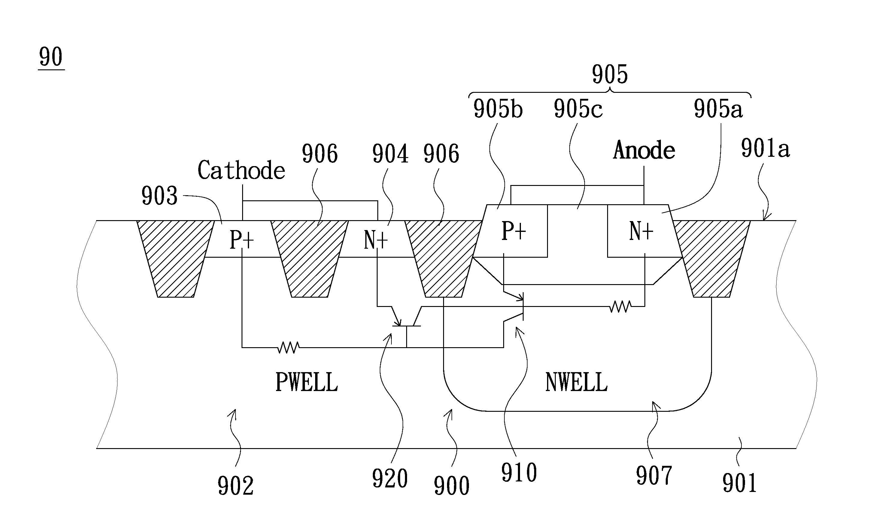
[0026]An improved semiconductor ESD protection apparatus device is provided in order to reduce a trigger voltage of a SCR device involved in the semiconductor ESD protection apparatus, whereby an improved ESD protection can be provided. The present invention will now be described more specifically with reference to the following embodiments. It is to be noted that the following descriptions of preferred embodiments of this invention are presented herein for the purpose of illustration and description only. It is not intended to be exhaustive or to be limited to the precise form disclosed.

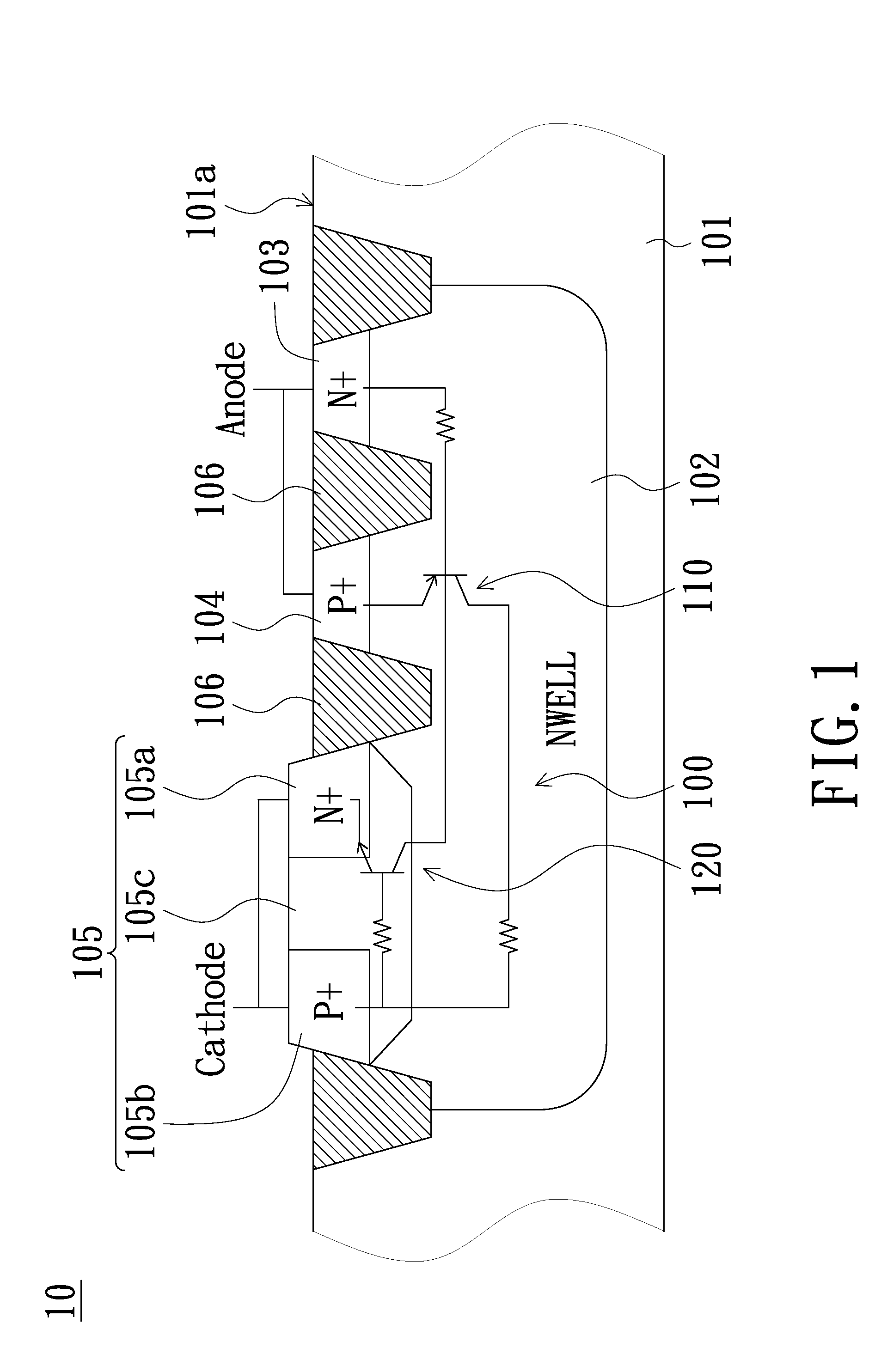
[0027]FIG. 1 is a cross-sectional view illustrating a semiconductor ESD protection apparatus 10 having a SCR device 100 in accordance with one embodiment of the present invention. The semiconductor ESD structure 10 comprises a substrate 101, a doped well 102, a doped area 103, a doped area 104 and an epitaxial layer 105. The substrate 101 is a P-type doped silicon substrate. The doped well 102 is do...


PUM


Abstract

A semiconductor ESD protection apparatus comprises a substrate; a first doped well disposed in the substrate and having a first conductivity; a first doped area having the first conductivity disposed in the first doped well; a second doped area having a second conductivity disposed in the first doped well; and an epitaxial layer disposed in the substrate, wherein the epitaxial layer has a third doped area with the first conductivity and a fourth doped area with the second conductivity separated from each other. Whereby a first bipolar junction transistor (BJT) equivalent circuit is formed between the first doped area, the first doped well and the third doped area; a second BJT equivalent circuit is formed between the second doped area, the first doped well and the fourth doped area; and the first BJT equivalent circuit and the second BJT equivalent circuit have different majority carriers.

Description

FIELD OF THE INVENTION[0001]The present invention relates to an electrostatic discharge (ESD) protection apparatus, and more particularly to a semiconductor ESD protection apparatus for integrated circuits (IC).BACKGROUND OF THE INVENTION[0002]An ESD event commonly results from the discharge of a high voltage potential and leads to pulses of high current in a short duration (typically, 100 nanoseconds). Semiconductor IC is vulnerable to ESD events resulted by human contact with the leads of the IC or electrically charged machinery being discharged in other leads of the IC. Accordingly, an ESD protection circuit is essential to a semiconductor IC.[0003]A parasitic silicon controlled rectifier (SCR) is one kind of on-chip semiconductor ESD protection device. Due to its high current sinking / sourcing capability, very low turn-on impedance, low power dissipation, and large physical volume for heat dissipating, parasitic lateral SCR devices have been recognized in the prior art as one of ...

Claims


Application Information

Patent Timeline
Patent Type & Authority Applications(United States)
IPC IPC(8): H02H9/04
CPCH01L29/7436H01L29/87H01L27/0262
Inventor WANG, CHANG-TZUTANG, TIEN-HAOSU, KUAN-CHENG
Owner UNITED MICROELECTRONICS CORP
Why Eureka
Try Eureka