Optical semiconductor modulator device and optical module
a technology of optical semiconductor and modulator device, which is applied in the direction of optics, optical light guides, instruments, etc., can solve the problems of difficult to raise the polarization extinction ratio, yield decline, and increase the loss of optical components, so as to achieve the effect of improving characteristics
- Summary
- Abstract
- Description
- Claims
- Application Information
AI Technical Summary
Benefits of technology
Problems solved by technology
Method used
Image

Examples
first embodiment
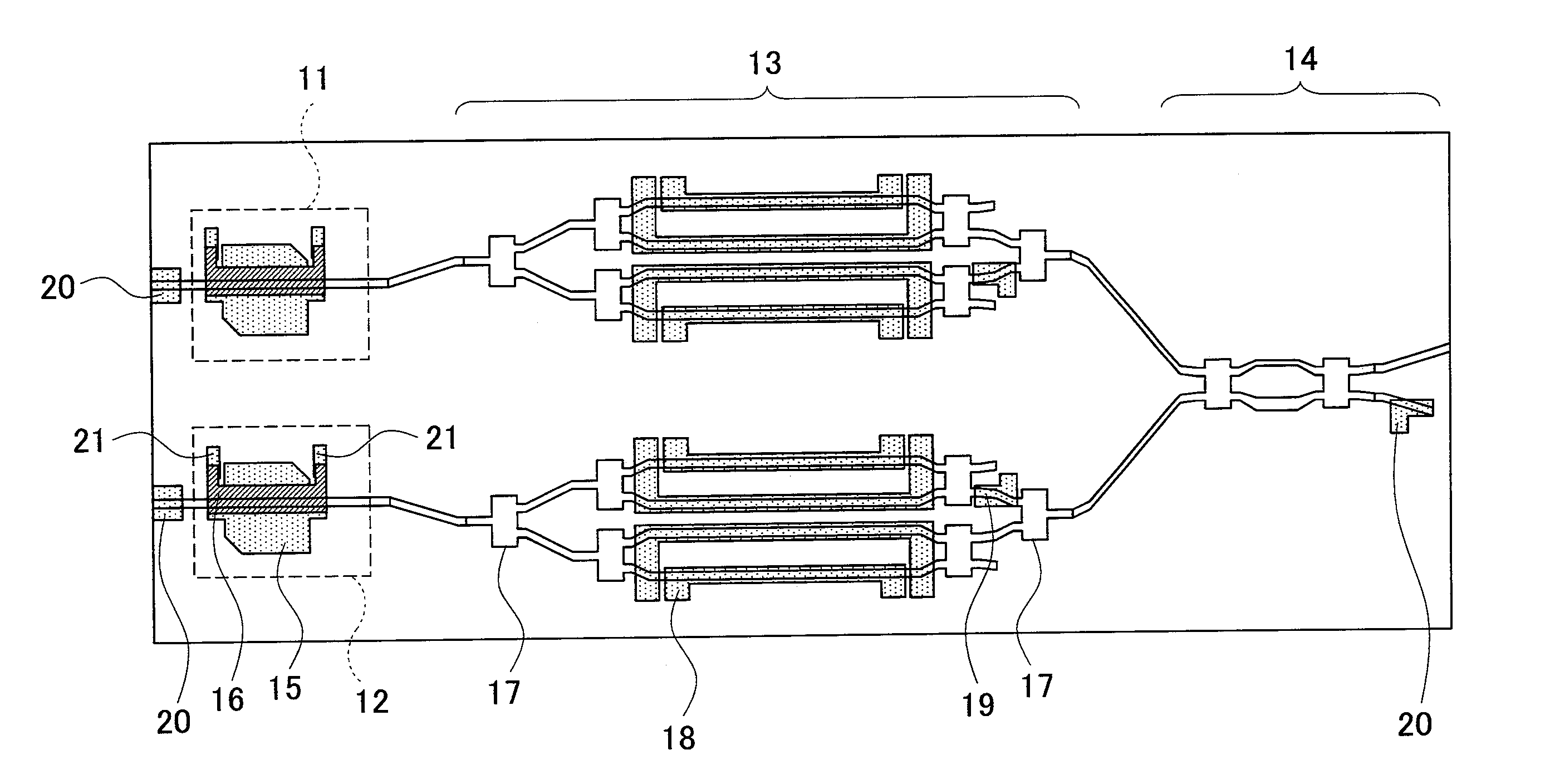
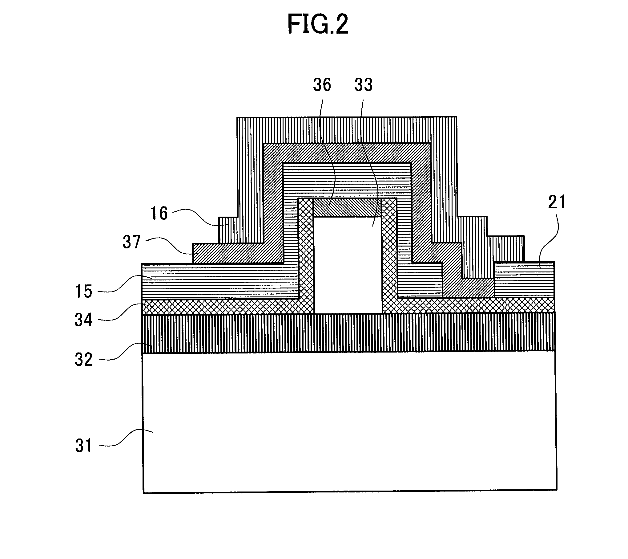
[0046]FIG. 1 is a schematic top view of an optical semiconductor device related to a first embodiment of the present invention. The optical semiconductor device related to the embodiment is a semiconductor optical integrated device in which two LDs, two QPSK modulators (modulation areas 13), a polarization multiplexer 14, and three PDs 20 are included on the same substrate. Herein the two LDs are a first LD 11 (a first light source) configured to output light having a TE polarization (a first polarization), and a second LD 12 (a second light source) configured to output light having a TM polarization (a second polarization), and both of them are distributed feedback type (DFB) LDs capable of adjusting the wavelength. In addition, the first LD 11 and the second LD 12 include a LD electrode 15 on a device surface thereof, and include a thin film resistor 16 formed by covering apart of the upper surface of the LD electrode 15. Two electrode pads 21 are provided on both ends of the thin...
second embodiment
[0074]An optical semiconductor device related to a second embodiment of the present invention differs from the optical semiconductor device related to the first embodiment in that an optical component for detecting whether there is a difference in the wavelengths of the two light sources is further included, but the others are the same configurations as those of the first embodiment. By including such an optical component, there is further an effect that the wavelength of the two light sources can be more precisely controlled in addition to the effect described in the first embodiment.
[0075]FIG. 5 is a schematic top view of the optical semiconductor device related to the present embodiment. On a side of each of the two LDs opposite to the modulation area 13 side, similarly to the PD 20 of the first embodiment, a first PD 40 serving as a light output monitor of the LD is placed so as to be optically connected to the corresponding LD. In addition, an optical waveguide 44 is further ex...
third embodiment
[0087]An optical semiconductor device related to a third embodiment of the present invention is different from the optical semiconductor device related to the second embodiment in that the location in which the ring resonator 42 and the optical waveguide are optically coupled to each other uses not the directional coupler but an MMI multiplexer / demultiplexer. However, the other structures are the same as those of the optical semiconductor device related to the second embodiment.
[0088]FIG. 6 is a schematic top view of the optical semiconductor device related to the present embodiment. As mentioned above, the MMI multiplexer / demultiplexer 45 is placed in the coupling location of the ring resonator 42 and the optical waveguide. The MMI multiplexer / demultiplexer 45 related to the present embodiment has a rectangular shape that is extended in an optical axial direction at a predetermined width by a predetermined length. In addition, the MMI multiplexers / demultiplexers 45 in which the opt...
PUM
| Property | Measurement | Unit |
|---|---|---|
| transmission distances | aaaaa | aaaaa |
| transmission distances | aaaaa | aaaaa |
| transmission distances | aaaaa | aaaaa |
Abstract
Description
Claims
Application Information
 - R&D
- Intellectual Property
- Life Sciences
- Materials
- Tech Scout
- Unparalleled Data Quality
- Higher Quality Content
- 60% Fewer Hallucinations
Browse by: Latest US Patents, China's latest patents, Technical Efficacy Thesaurus, Application Domain, Technology Topic, Popular Technical Reports.
© 2025 PatSnap. All rights reserved.Legal|Privacy policy|Modern Slavery Act Transparency Statement|Sitemap|About US| Contact US: help@patsnap.com