Light emission apparatus and manufacturing method thereof

Inactive Publication Date: 2013-08-15
OCEANS KING LIGHTING SCI&TECH CO LTD
View PDF0 Cites 1 Cited by
  • Summary
  • Abstract
  • Description
  • Claims
  • Application Information

AI Technical Summary

Benefits of technology

[0016]2. In the method for manufacturing the luminescent device of the present invention, the luminescent device is produced simply by disposing a m

Problems solved by technology

However, when used as a luminescent material in a field emission device, t

Method used


Image

  • Light emission apparatus and  manufacturing method thereof
  • Light emission apparatus and  manufacturing method thereof
  • Light emission apparatus and  manufacturing method thereof

Examples


example 1

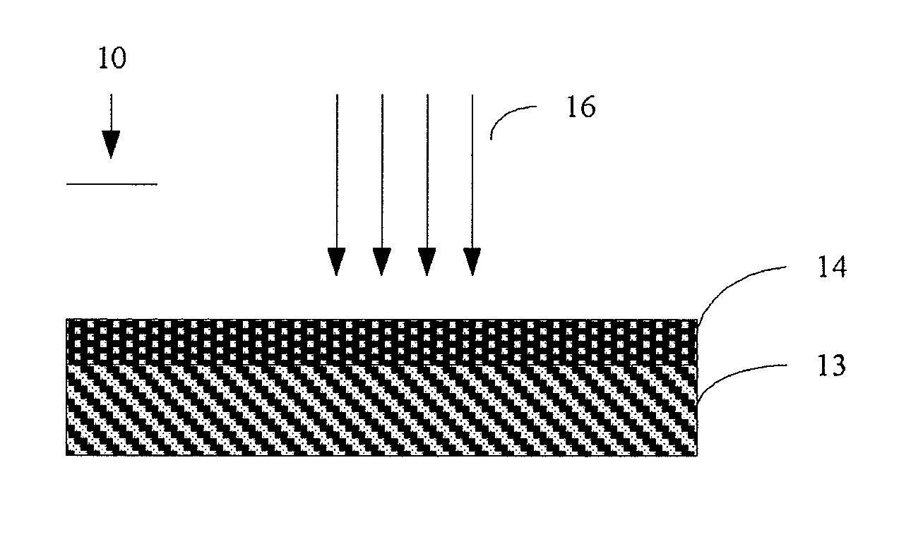
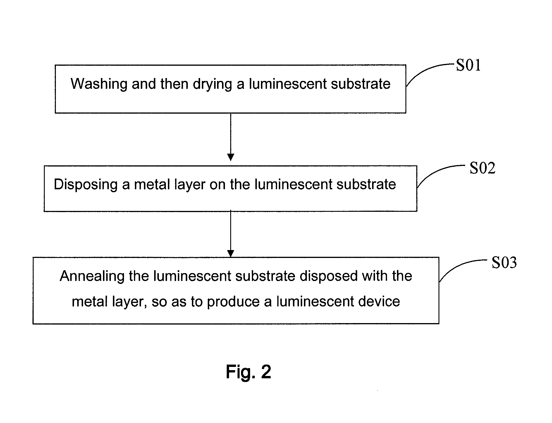
[0036]A Tb-doped yttrium aluminum garnet series transparent ceramic plate, i.e. a luminescent ceramic having a formula of Y3Al5O12:Tb, is used as the luminescent substrate. A silver layer having a thickness of 10 nm is deposited on a surface of the transparent ceramic plate with a magnetron sputtering equipment. The resulted device is placed in a vacuum environment have a vacuity of −3 Pa, annealed at 300° C. for half an hour, and then cooled to room temperature, to give a luminescent device with a metal layer having a metal microstructure.

[0037]A spectral test is carried out on the luminescent device manufactured above, wherein the luminescent device is bombarded by cathode rays produced by an electron gun. An electron beam first passes through the metal layer and then excites transparent ceramic Y3Al5O12:Tb to emit light, yielding a luminescent spectrum as shown in FIG. 4. The spectrum in the figure shows that the luminescent material is a green-light-emitting luminescent material...

example 2

[0038]Example 2 is basically the same as Example 1, excepted that a gold layer having a thickness of 0.5 nm is deposited on a surface of the luminescent substrate, the resulted device is placed in a vacuum environment have a vacuity of −3 Pa, annealed at 650° C. for 1 hour, and then cooled to room temperature, to give a luminescent device with a metal layer having a metal microstructure.

example 3

[0039]Example 3 is basically the same as Example 1, excepted that an aluminum layer having a thickness of 200 nm is deposited on a surface of the luminescent substrate, the resulted device is placed in a vacuum environment have a vacuity of −3 Pa, annealed at 50° C. for 5 hours, and then cooled to room temperature, to give a luminescent device with a metal layer having a metal microstructure.


PUM

PropertyMeasurementUnit
Temperatureaaaaaaaaaa
Thicknessaaaaaaaaaa

Abstract

A light emission apparatus (10) and a manufacturing method thereof are provided. The light emission apparatus includes a light emission base body (13) and a metal layer (14) with metal microstructure. The metal layer is set on the surface of the light emission base body. The material of light emission base body is transparent ceramic Y3Al5O12:Tb. By setting a metal layer with metal microstructure on the light emission base body, the interface between the metal layer and the light emission base body could form a surface plasmon under the cathode ray (16). The spontaneous emission of the transparent ceramic and the emission efficiency of the light emission base body could be enhanced by the effect of surface plasmon.

Description

TECHNICAL FIELD[0001]The present invention relates to the technical field of luminescent materials, and particularly to a luminescent device. The present invention also relates to a method for manufacturing a luminescent device.BACKGROUND ART[0002]Conventional materials used as the luminescent substrate include fluorescent powder, nano-crystal, luminescent glass, transparent ceramic, and the like. Transparent ceramic has distinctive advantages over other luminescent materials. Compared with luminescent glass, transparent ceramic has higher luminescent efficiency. Compared with fluorescent powder and nano-crystal, transparent ceramic has characteristics of transparency, high mechanical strength, good chemical stability, etc., and is easier to be processed into products with various sizes and shapes, such as displays or illumination lighting sources with various sizes or shapes.[0003]For example, in the field of vacuum microelectronics, luminescent ceramic is usually used as phosphor ...

Claims


Application Information

Patent Timeline
IPC IPC(8): H01J1/63H01J9/00
CPCH01J1/63Y10T428/265C04B2235/3224C04B2235/3225C23C14/185B82Y20/00C04B35/44C09K11/7749C23C14/35C23C14/5806H01J9/20H01J31/127H01J63/04C04B2235/764C04B2235/9653H01J9/00
Inventor ZHOU, MINGJIEMA, WENBOLIU, YUGANG
Owner OCEANS KING LIGHTING SCI&TECH CO LTD
Why Eureka
Try Eureka