Carbon nanotube field emission devices and methods of making same
- Summary
- Abstract
- Description
- Claims
- Application Information
AI Technical Summary
Benefits of technology
Problems solved by technology
Method used
Image
Examples
examples
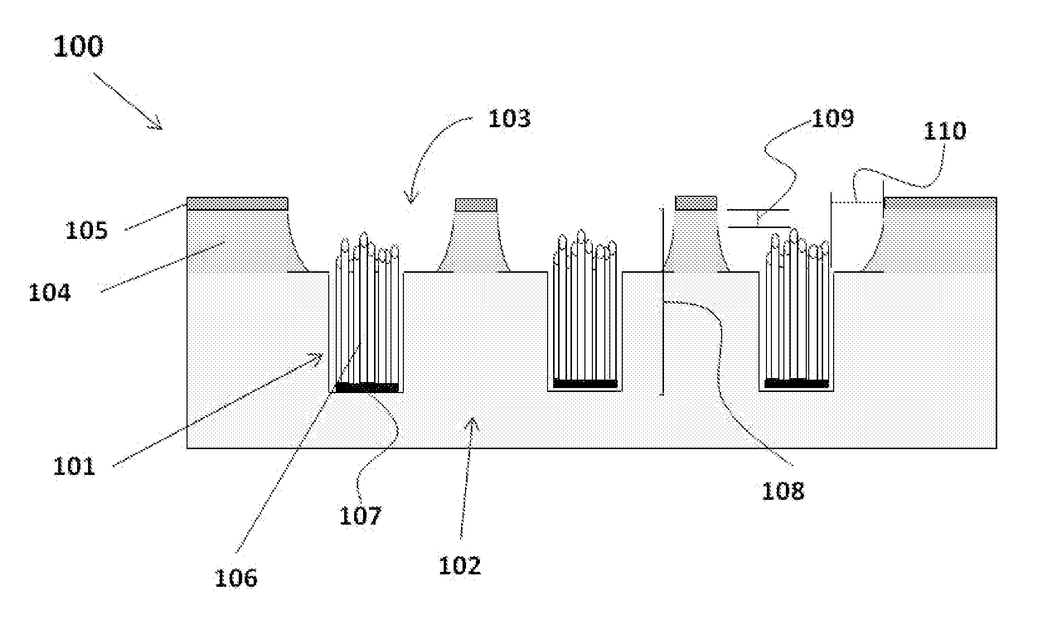
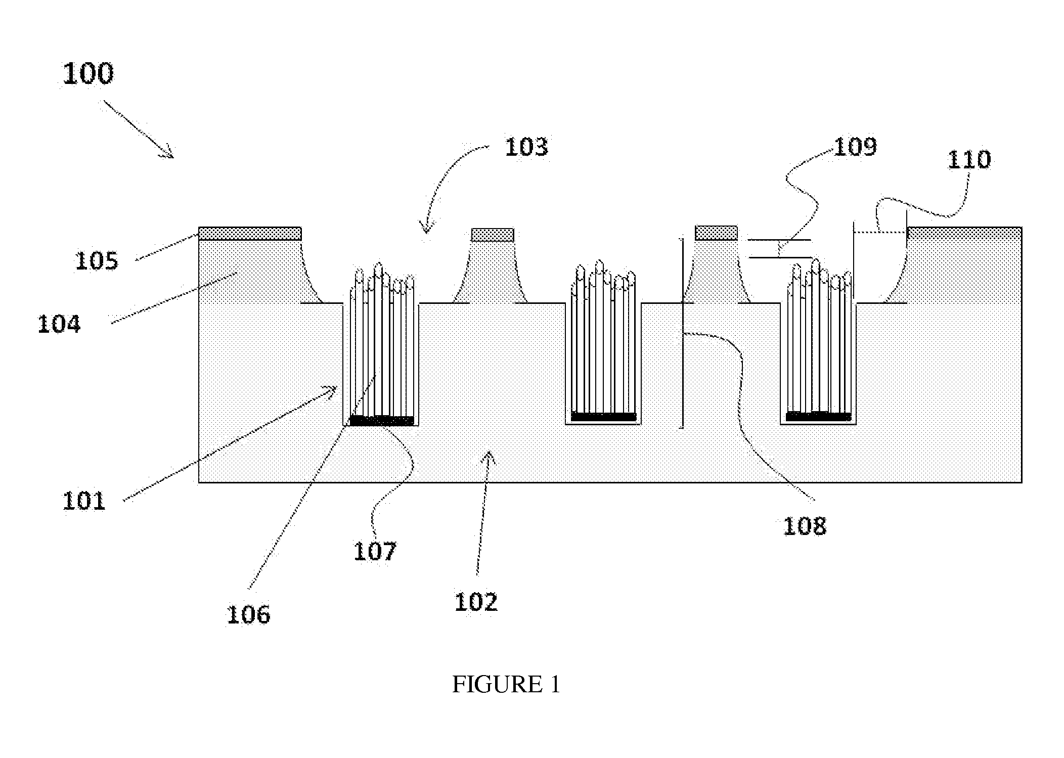
[0092]Arsenic-doped silicon wafers with a resistivity of 0.001-0.005 Ωcm serve as the substrate and cathode contact.
[0093]Thermally grown SiO2 synthesized at 1100° C. for ˜24 h is used as the insulator and doped polycrystalline silicon (p-Si) is used as the gate. The 500 nm p-Si is deposited by low pressure chemical vapour deposition (LPCVD) at 588° C. and 250 mTorr with a silane flow of 100 sccm for 90 min The p-Si is doped with Techneglas (Perrysburg, Ohio) PhosPlus TP-470 solid source dopant by heating to 1050° C. for 1 h followed by a drive-in anneal at 1100° C. for 30 min These particular materials are chosen to maximize film quality while maintaining ease of fabrication. Thermal oxide deposits the best quality SiO2 in terms of density, uniformity, purity, and dielectric breakdown. It has a theoretical dielectric breakdown of about 1000 V μm−1, which can be 10 times higher than CVD SiO2. High dielectric breakdown prevents degradation of the device during operation. The p-Si is ...
PUM
 Abstract
Description
Claims
Application Information
 - R&D Engineer
- R&D Manager
- IP Professional
- Industry Leading Data Capabilities
- Powerful AI technology
- Patent DNA Extraction
Browse by: Latest US Patents, China's latest patents, Technical Efficacy Thesaurus, Application Domain, Technology Topic, Popular Technical Reports.
© 2024 PatSnap. All rights reserved.Legal|Privacy policy|Modern Slavery Act Transparency Statement|Sitemap|About US| Contact US: help@patsnap.com


