

Method for the reuse of gallium nitride epitaxial substrates
- Summary
- Abstract
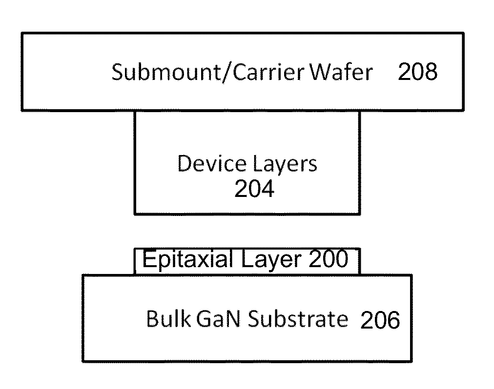
- Description
- Claims
- Application Information
AI Technical Summary
Benefits of technology
Problems solved by technology
Method used
Image

Examples
example
Vertical Cavity Surface Emitting Laser (VCSEL)
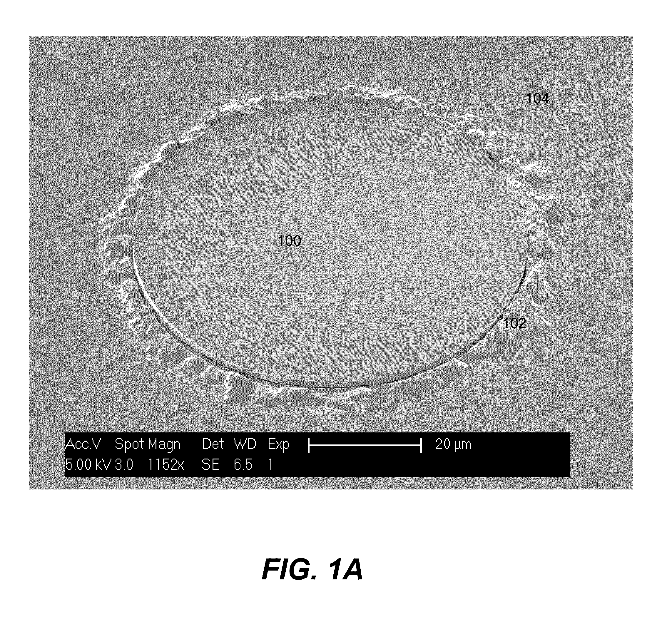
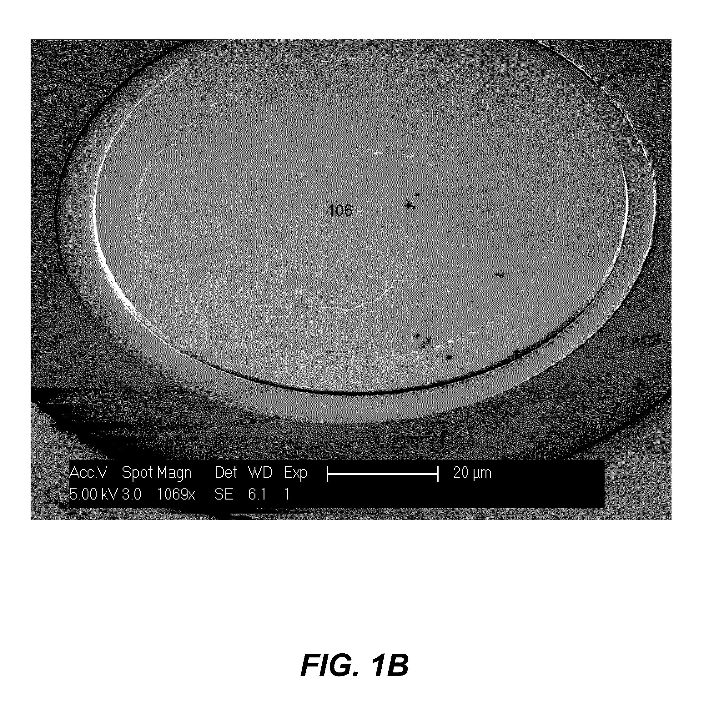
[0070]FIG. 4(a) shows a schematic illustration of the VCSEL device structure. The epitaxial structure was grown on a free-standing m-plane GaN substrate (nominally offcut by 1° in the -c-direction) using atmospheric-pressure metal-organic chemical vapor deposition. The active region is aligned with a peak of the optical standing wave and consists of 5 In0.10Ga0.90N (7 nm) quantum wells with GaN (5 nm) barriers and a 15 nm Mg-doped Al0.20Ga0.80N electron blocking layer. An additional region of 3 In0.12Ga0.88N (7 nm) quantum wells with GaN (5 nm) barriers was embedded in the n-GaN beneath the active region (sacrificial layer). This region was laterally undercut using band-gap-selective PEC etching after flip-chipping to separate the substrate from the devices. The placement of a 15 nm Al0.30Ga0.70N hole-blocking layer 50 nm above the sacrificial region served to define the cavity length (7.5 k) and to prevent hole transport to the device s...
PUM
 Abstract
Description
Claims
Application Information