
Dielectrics using substantially longitudinally oriented insulated conductive wires

a technology of conductive wires and dielectrics, applied in the field of conductive wires, can solve the problems of limited application and use of existing artificial dielectrics, limited ability to achieve high dielectric constants within existing artificial dielectrics, and limited application of dielectric structures based on existing dielectrics. achieve the effect of improving the performance of cell phones

Inactive Publication Date: 2013-09-19
NANOSYS INC
View PDF2 Cites 23 Cited by
  • Summary
  • Abstract
  • Description
  • Claims
  • Application Information

AI Technical Summary

Benefits of technology

This patent discusses the use of dielectric materials in electronic devices to improve performance. These materials can be used in devices like capacitors, thin film transistors, and filters, among others. The patent focuses on the benefits of using these materials in devices that communicate with radio waves, such as cell phones and computers. The technical effects of the patent text are that dielectric materials can improve the performance of electronic devices and enhance their overall function and efficiency.

Problems solved by technology

Existing artificial dielectrics are limited in their application and use because they typically have relatively low dielectric constants and have fixed dielectric constants at a particular frequency.
These limitations, as discussed in Stockton, have been attributed to clumping of metallized fibers once the density of the fibers becomes high.
When the metallized fibers clump, they lose their insulative characteristics and become conducting, thereby limiting the ability to achieve high dielectric constants within existing artificial dielectrics.
Furthermore, dielectric structures based on existing dielectrics and dielectric structures are limited in their application.

Method used


Image

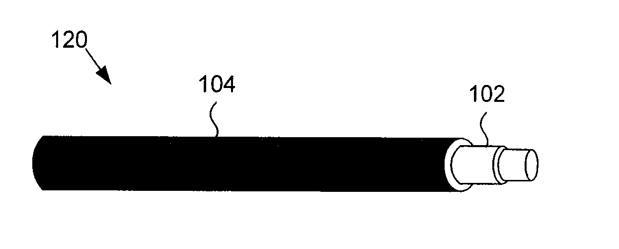
  • Dielectrics using substantially longitudinally oriented insulated conductive wires
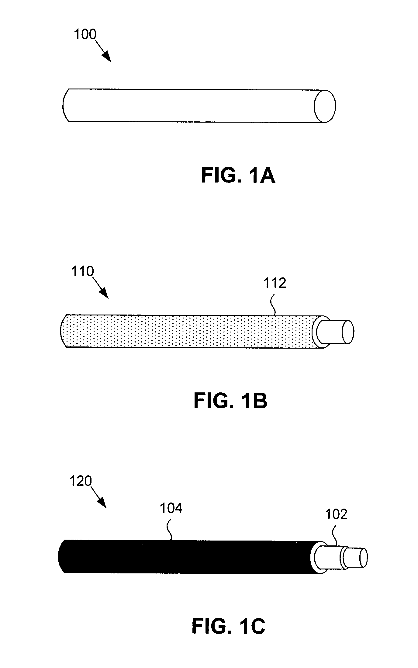
  • Dielectrics using substantially longitudinally oriented insulated conductive wires
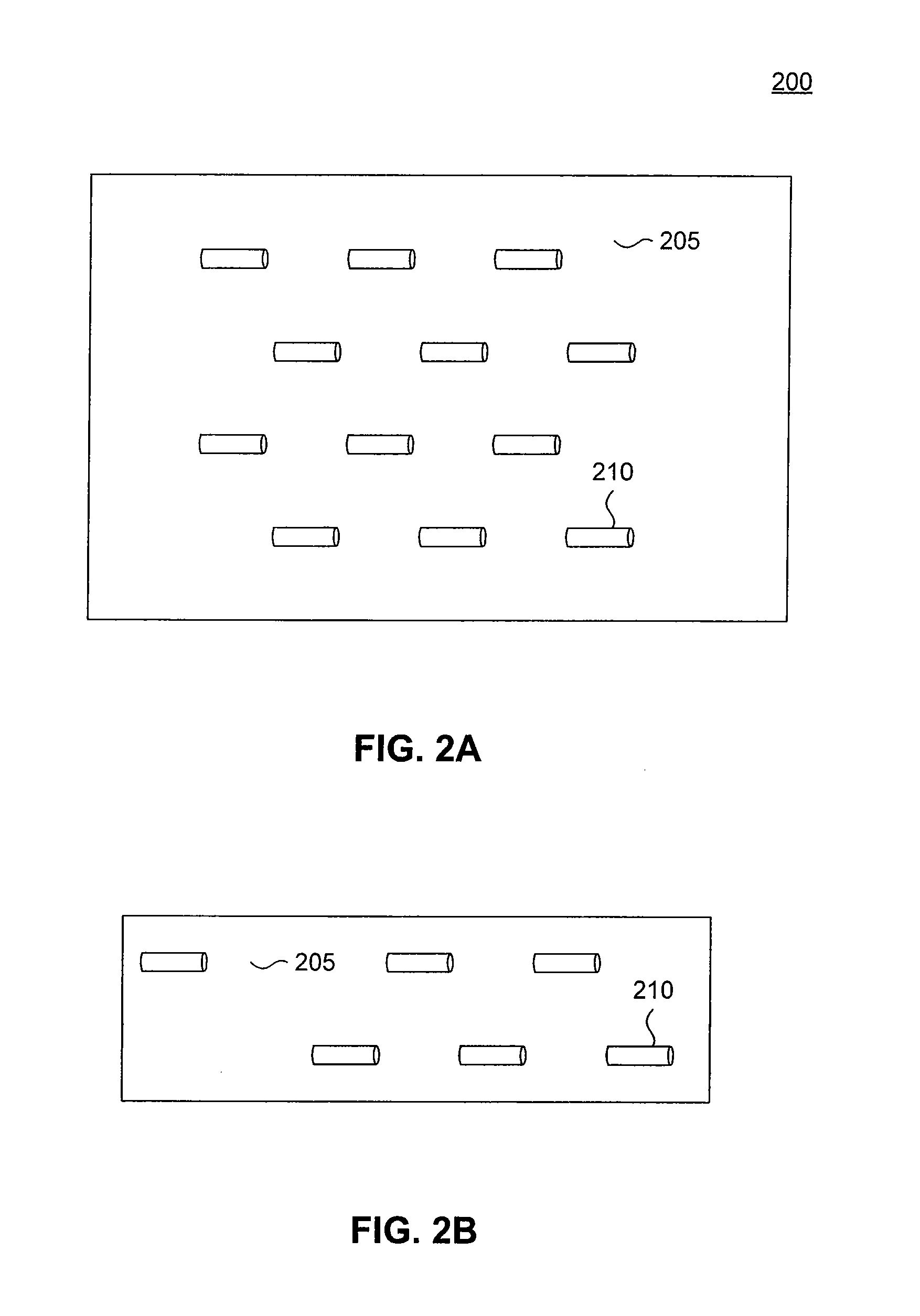
  • Dielectrics using substantially longitudinally oriented insulated conductive wires

Examples


example

[0169]75 / 50 SPNSN wire was obtained from MWS wire industries. This product consists of 75 strands of polyurethane-nylon insulated 50 gauge copper wire. Approximately 50 two centimeter lengths of the stranded wire were placed longitudinally into a three centimeter piece of heat shrink tubing. The tubing was activated with a hot air gun and shrunk conformably around the wire bundle. About 1 cm was sliced of each end of the bundle. The center piece was then placed into a vial containing uncured epoxy. The vial was placed into a vacuum chamber and evacuated until bubbles could no longer be observed coming out of the epoxy. The vacuum was broken and the wire bundle was then placed in an oven at 80 degrees Celsius to cure the epoxy that had filled the voids between the wires. After curing a transverse 3 mm slice was taken out of the bundle with a razor blade. Teflon films were then placed on the ends of the piece and dielectric measurements were performed. The dielectric constant of the m...


PUM

PropertyMeasurementUnit
Pore sizeaaaaaaaaaa
Thicknessaaaaaaaaaa
Diameteraaaaaaaaaa

Abstract

A dielectric material is disclosed comprising a plurality of substantially longitudinally oriented wires which are coupled together, wherein each of the wires includes a conductive core comprising a first material and one or more insulating shell layers comprising a compositionally different second material disposed about the core. In one embodiment, a dielectric layer is disclosed comprising a substrate comprising an insulating material having a plurality of nanoscale pores defined therein having a pore diameter less than about 100 nm, and a conductive material disposed within the nanoscale pores. Methods are also disclosed to create a dielectric material layer comprising, for example, providing a plurality of wires, wherein each of the wires includes a core comprising a first material and one or more insulating layers comprising a compositionally different second material disposed about the core; substantially longitudinally orienting said plurality of wires along their long axes; coupling the wires together; and depositing an insulating coating on at least one of a top and / or a bottom end of the wires.

Description

CROSS REFERENCE TO RELATED APPLICATIONS[0001]The present application is a continuation-in-part to U.S. patent application Ser. No. 11 / 589,988 entitled Continuously Variable Graded Artificial Dielectrics Using Nanostructures, filed Oct. 31, 2006, which is a continuation-in-part to U.S. patent application Ser. No. 11 / 203,432, entitled Artificial Dielectrics Using Nanostructures, filed on Aug. 15, 2005 by Stumbo et. al. (“432 Application”), which are each hereby expressly incorporated by reference.[0002]The '432 Application claims priority to U.S. Provisional Patent Application No. 60 / 610,219, entitled Artificial Dielectrics Using Nanostructures, filed on Sep. 16, 2004 by Stumbo et. al., which is hereby expressly incorporated by reference in its entirety.BACKGROUND OF THE INVENTION[0003]1. Field of the Invention[0004]The invention relates to nanowires, and more particularly to controllable artificial dielectrics using nanowires.[0005]2. Background Art[0006]Dielectrics are materials tha...

Claims


Application Information

Patent Timeline
IPC IPC(8): H01B7/00H01G4/018
CPCH01B3/004H01G4/20H01G4/018H01B7/0009B82Y99/00Y10T428/249924
Inventor DUBROW, ROBERT S.MILLER, JEFFREYSTUMBO, DAVID P.
Owner NANOSYS INC
Learn More