Semiconductor photocathode and method for manufacturing the same

a technology of semiconductors and photocathodes, applied in the manufacture of electrode systems, electric discharge tubes/lamps, tubes with screens, etc., can solve the problems of comparatively low quantum efficiency, strong wavelength dependence, and insufficient sensitivities (quantum efficiencies) of semiconductors, and achieve the effect of increasing quantum efficiency and easy production

Active Publication Date: 2013-09-26
SANKEN ELECTRIC CO LTD +1
View PDF5 Cites 12 Cited by
  • Summary
  • Abstract
  • Description
  • Claims
  • Application Information

AI Technical Summary

Benefits of technology

[0033]According to the present semiconductor photocathode, the quantum efficiency becomes higher than t

Problems solved by technology

A conventionally known photocathode with a CsTe layer or a CsI layer can be used for detection of far-ultraviolet rays but is comparatively low in quantum efficiency and has strong wavelength dependence.
In both semicon

Method used


Image

  • Semiconductor photocathode and method for manufacturing the same
  • Semiconductor photocathode and method for manufacturing the same
  • Semiconductor photocathode and method for manufacturing the same

Examples


case 1

[0310]( refer to Type 2)[0311]In the region 0≦x2+DM:[0312]X=g(x)=(X2−X1)×(1−x / (D2+DM))+X1 is satisfied, and[0313]in the region D2+DM≦x2+DM+D1:[0314]X=g(x)=X1 or[0315]X=g(x)≦X1 is satisfied.

case 2

[0316]( refer to Type 3)[0317]In the region 0≦x2:[0318]X=g(x)=X2, or[0319]X=g(x)≧X2 is satisfied,[0320]in the region D2≦x2+DM:[0321]X=g(x)=−(X2−X1)×(x−D2) / DM+X2 is satisfied, and[0322]in the region D2+DM≦x2+DM+D1:[0323]X=g(x)=X1 or[0324]X=g(x)≦X1 is satisfied.

case 3

[0325]( refer to Type 3)[0326]In the region 0≦x2:[0327]X=g(x)=X2, or[0328]X=g(x)≧X2 is satisfied,[0329]in the region D2≦x2+DM:[0330]X=g(x)=(X2−X1) ×(e−x / (D2+DM)−e−1) / (1−e−1)+X1 is satisfied, and[0331]in the region D2+DM≦x2+DM+D1:[0332]X=g(x)=X1, or[0333]X=g(x)≦X1 is satisfied.

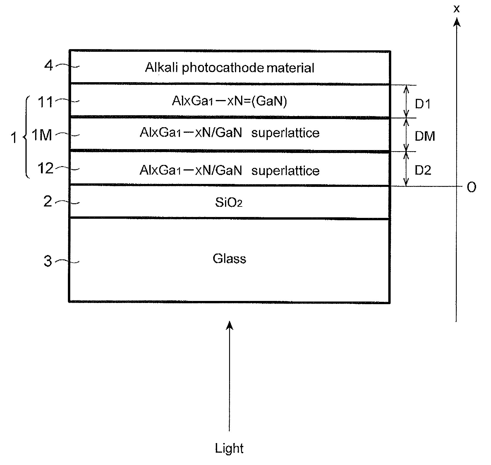
[0334]The composition ratio X at each position can include an error of ±10%. In the case of the above functions, the quantum efficiency can be improved because the energy for the region on the glass substrate side can be raised from the position of the peak of the energy in the lower end of the conduction band. The thickness D2 satisfies a substantially equal (error: ±50%) relationship (D2=DM±DM×50%) with the thickness DM. In the above embodiment, the intermediate region 1M, the first region 11, and the second region 12 are in contact with one another, however, an AlGaN layer which does not affect the characteristic can also be provided among them.


PUM


Abstract

A semiconductor photocathode includes an AlXGa1-XN layer (0≦X<1) bonded to a glass substrate via an SiO2 layer and an alkali-metal-containing layer formed on the AlXGa1-XN layer. The AlXGa1-XN layer includes a first region, a second region, an intermediate region between the first and second regions. The second region has a semiconductor superlattice structure formed by laminating a barrier layer and a well layer alternately, the intermediate region has a semiconductor superlattice structure formed by laminating a barrier layer and a well layer alternately. When a pair of adjacent barrier and well layers is defined as a unit section, an average value of a composition ratio X of Al in a unit section decreases monotonously with distance from an interface position between the second region and the SiO2 layer at least in the intermediate region.

Description

BACKGROUND[0001]1. Technical Field Modes of the present invention relate to a semiconductor photocathode that emits electrons in response to incident light and a method for manufacturing the same.[0002]2. Related Background Art[0003]A conventionally known photocathode with a CsTe layer or a CsI layer can be used for detection of far-ultraviolet rays but is comparatively low in quantum efficiency and has strong wavelength dependence. In contrast, a photocathode using a compound semiconductor has potential for an improvement in these disadvantages.[0004]Recent semiconductor photocathodes are described in Patent Document 1 and Patent Document 2. In Patent Document 1, a GaN layer is grown on a sapphire substrate to obtain a GaN layer of high quality. The GaN layer can be grown on a c-plane of the sapphire substrate. In both semiconductor photocathodes, a transparent substrate and a GaN layer are used and although both are capable of emitting electrons in response to incident light, sens...

Claims


Application Information

Patent Timeline
IPC IPC(8): H01J1/308H01J9/02
CPCH01J1/308H01J9/025H01J31/507H01J9/12H01J1/34H01J31/26
Inventor FUKE, SHUNROMATSUO, TETSUJIISHIGAMI, YOSHIHIRONIHASHI, TOKUAKI
Owner SANKEN ELECTRIC CO LTD
Why Eureka
Try Eureka