Processor and electronic device

a technology of electronic devices and processors, applied in the field of processors, can solve the problems of increasing power consumption and reducing power consumption insufficient amounts, and achieve the effect of reducing power consumption

Inactive Publication Date: 2013-10-03
SEMICON ENERGY LAB CO LTD
View PDF18 Cites 17 Cited by
  • Summary
  • Abstract
  • Description
  • Claims
  • Application Information

AI Technical Summary

Benefits of technology

[0010]An object of one embodiment of the present invention is to reduce power consumption.

Problems solved by technology

Therefore, in an instruction execution period for example, when clock gating or power gating is carried out in the case where the supply of a clock signal and a power source voltage is stopped for a short period of time, power consumption rather increases in some cases, which has not led to a sufficient reduction in power consumption.

Method used


Image

  • Processor and electronic device
  • Processor and electronic device
  • Processor and electronic device

Examples


embodiment 1

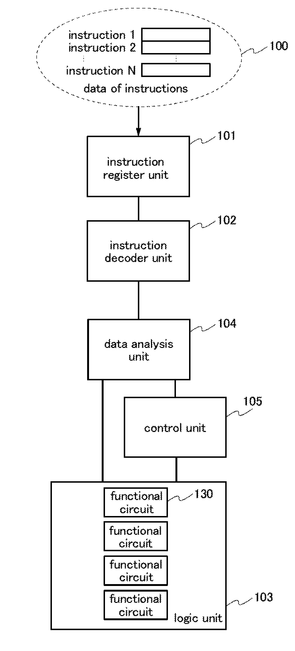
[0036]In this embodiment, an example of a processor will be described.

[0037]FIG. 1 shows an example of a configuration of the processor of this embodiment.

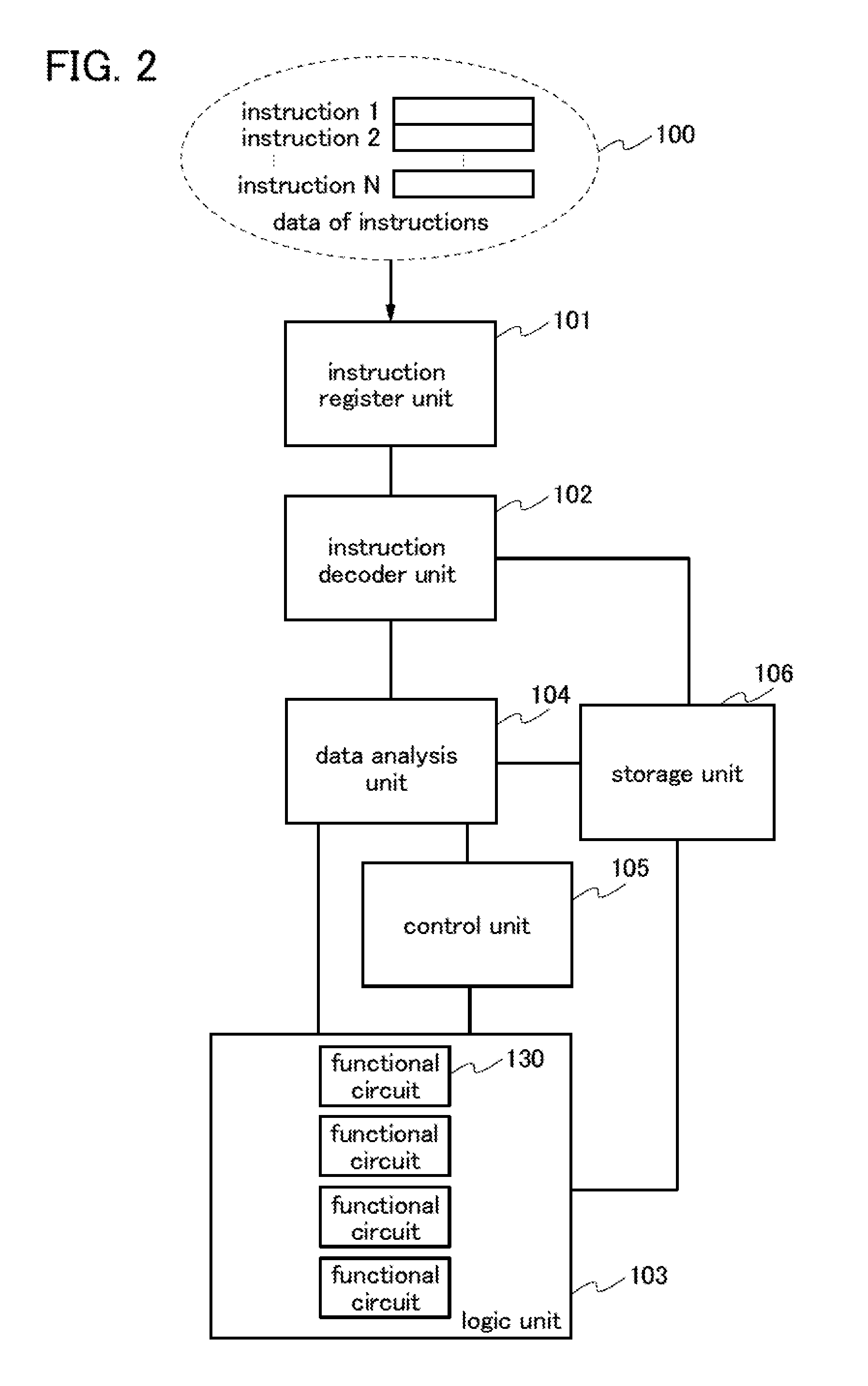
[0038]The processor shown in FIG. 1 includes an instruction register unit 101, an instruction decoder unit 102, a logic unit 103, a data analysis unit 104, and a control unit 105. Note that as shown in FIG. 2, a storage unit 106 may be provided to read or write data from or to each of the instruction decoder unit 102, the logic unit 103, and the data analysis unit 104. The storage unit 106 is provided with a plurality of registers including a register file, an accumulator, a program counter, a flag register, and the like.

[0039]Data 100 of sequential instructions is fetched in the instruction register unit 101. The instruction register unit 101 has a function of storing data of instructions to be translated. The instruction decoder unit 102 has a function of decoding each data of instructions which has been fetched in the instructi...

embodiment 2

[0157]Described in this embodiment is an example of a configuration of a register which can be used for the processor of one embodiment of the present invention.

[0158]FIGS. 12A and 12B show an example of the configuration of the register of this embodiment.

[0159]The register shown in FIG. 12A includes a flip-flop (also referred to as FF) 201, a memory circuit (also referred to as NVM) 202, and a selector (also referred to as SEL) 203. Note that the flip-flop 201 and the memory circuit 202 may be considered as one memory circuit, and the register may include a plurality of memory circuits.

[0160]The flip-flop 201 is supplied with a reset signal RST, a clock signal CLK, and a data signal. The flip-flop 201 has a function of holding data of the data signal that is input in response to the clock signal CLK and outputting the data as a data signal Q.

[0161]The memory circuit 202 is supplied with a write control signal WE, a read control signal RD, and a data signal.

[0162]The memory circuit...

embodiment 3

[0215]In this embodiment, examples of a structure of a transistor which can be used in one embodiment of the present invention will be described with reference to schematic cross-sectional views of FIGS. 15A and 15B. Note that components shown in FIGS. 15A and 15B are not to scale in some cases.

[0216]A transistor shown in FIG. 15A includes a conductive layer 711, an insulating layer 712, a semiconductor layer 713, conductive layers 717a and 717b, and insulating layers 718a and 718b.

[0217]The semiconductor layer 713 is provided over an element formation layer 700 with an insulating layer 703 interposed therebetween. Note that the semiconductor layer 713 is not necessarily provided over the insulating layer 703 and may be provided directly on the element formation layer 700.

[0218]In the semiconductor layer 713, a region 715a and a region 715b to which a dopant is added are provided separately from each other. Moreover, in the semiconductor layer 713, a region 716a and a region 716b t...


PUM


Abstract

Power consumption is reduced. A processor includes an instruction register unit in which data of a plurality of instructions is fetched; an instruction decoder unit in which each of the plurality of instructions is translated; a logic unit including a functional circuit which is supplied with a clock signal and a power source voltage, supplied with a data signal including the translated data of the instructions, and operates in accordance with the supplied data of the instructions; a data analysis unit in which the translated data is analyzed so as to calculate a non-operating period of the functional circuit, and a control signal is generated; and a control unit which controls the supply of the clock signal or both the clock signal and the power source voltage to the functional circuit in accordance with the control signal.

Description

TECHNICAL FIELD[0001]The present invention relates to a processor. The present invention also relates to an electronic device including the processor.BACKGROUND ART[0002]In recent years, techniques for reducing the power consumption of processors have been developed.[0003]The reduction in power consumption is realized by clock gating or power gating, for example.[0004]The clock gating is a technique for controlling the supply of a clock signal to a circuit so as to stop the supply of the clock signal to, for example, a circuit which is not in use.[0005]The power gating is a technique for controlling the supply of a power source voltage to a circuit so as to stop the supply of the power source voltage to, for example, a circuit which is not in use.[0006]The aforementioned clock gating and power gating are performed in accordance with, for example, instruction data input to a processor (see Patent Document 1, for example).REFERENCEPatent Document[0007][Patent Document 1] Japanese Publ...

Claims


Application Information

Patent Timeline
Patent Type & Authority Applications(United States)
IPC IPC(8): G06F1/32
CPCG06F1/324Y02B60/1221G06F1/3237Y02D10/00
Inventor YONEDA, SEIICHI
Owner SEMICON ENERGY LAB CO LTD
Why Eureka
Try Eureka