Tandem White Organic Light Emitting Device

a light-emitting device and organic technology, applied in the direction of organic semiconductor devices, electric vehicle charging technology, thermoelectric devices, etc., can solve the problems of inability to transport holes or electrons of the charge generation layer into adjacent stacks, complicating the manufacturing process, and conventional white organic light-emitting devices as described, etc., to achieve long life and high efficiency

Active Publication Date: 2013-10-10
LG DISPLAY CO LTD
View PDF7 Cites 42 Cited by
  • Summary
  • Abstract
  • Description
  • Claims
  • Application Information

AI Technical Summary

Benefits of technology

[0018]An object of the present invention is to provide a tandem white organic light emitting device having high effic

Problems solved by technology

However, conventional white organic light emitting devices as described above have the following problems.
However, in the tandem white organic light emitting device, holes or electrons of the charge generation layer may not be transp

Method used


Image

  • Tandem White Organic Light Emitting Device
  • Tandem White Organic Light Emitting Device
  • Tandem White Organic Light Emitting Device

Examples


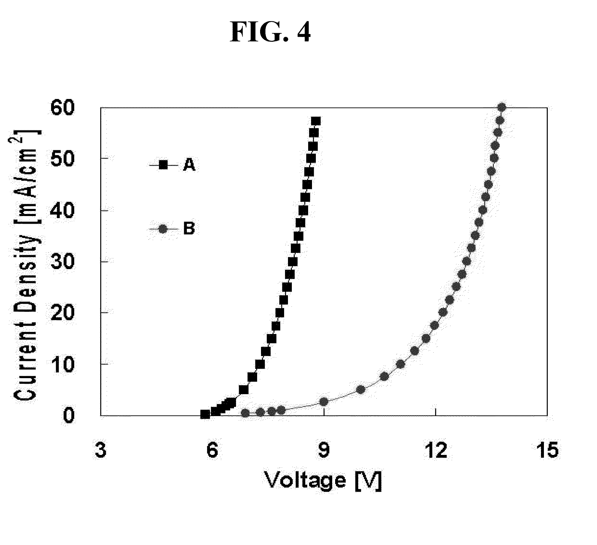
experimental example

of Device D

[0117]Hereinafter, formation of the tandem white organic light emitting device D according to the present invention will be briefly described.

[0118]However, this is an example, and materials described below are not limited thereto. Any other materials may also be used as long as the materials maintain functions of the layers.

[0119]A thin film transistor array including a thin film transistor (not shown) aligned in each of the pixels in a matrix form is formed on a transparent substrate (not shown).

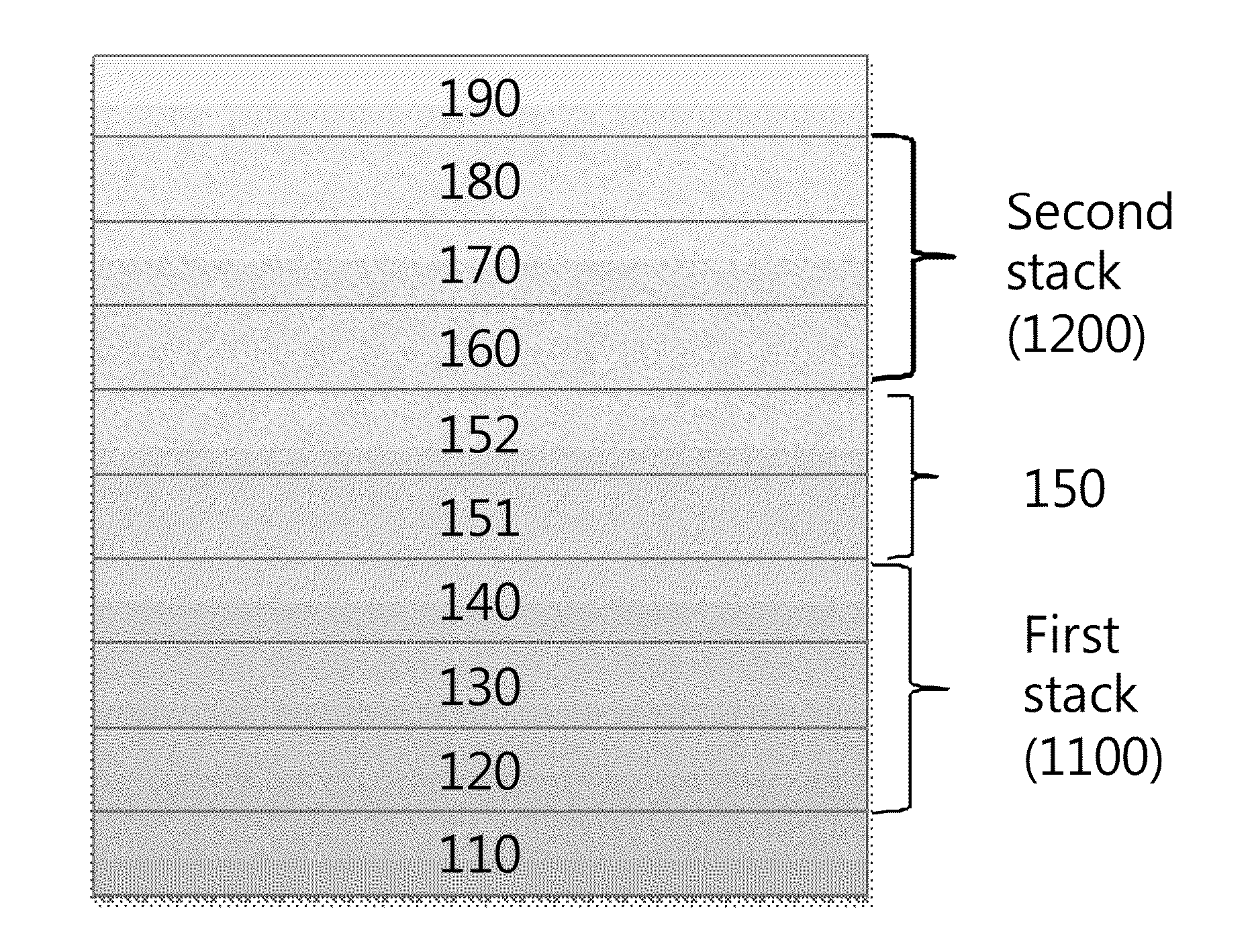
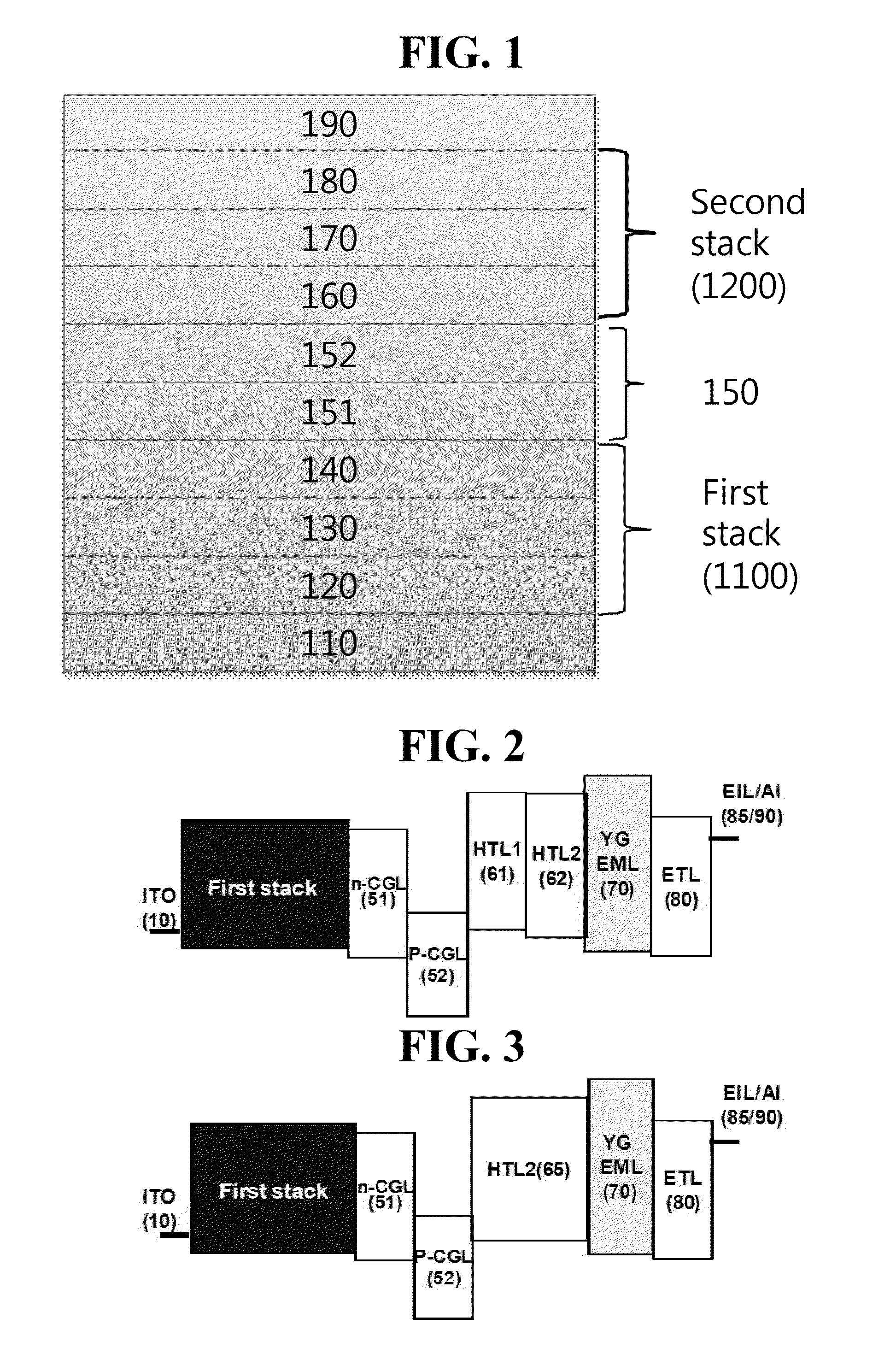
[0120]Then, as shown in FIGS. 1 and 8, a first electrode 110 is formed using an anode material to be in contact with the thin film transistor. Indium tin oxide (ITO) is generally used as the anode material.

[0121]Then, a first hole transport layer 120 is formed on the first electrode 110. The first hole transport layer 120 is formed by continuously depositing HAT-CN (Formula 1) to a thickness of 50 Å, 4,4′-bis[N-1-naphthyl)-N-phenylamino]-biphenyl (NPD, Formula 2) and N,N′-diphen...


PUM


Abstract

A tandem white organic light emitting device having high efficiency and long lifespan by adjusting characteristics of a hole transport layer adjacent to a charge generation layer consisting of p-type and n-type charge generation layer is disclosed, the p-type charge generation layer is formed of organic materials only, and at least one organic material contained in the p-type charge generation layer has a LUMO level of −6.0 eV to −4.5 eV.

Description

[0001]This application claims the benefit of Korean Patent Application No. 10-2012-0035336, filed on Apr. 5, 2012, which is hereby incorporated by reference as if fully set forth herein.BACKGROUND OF THE INVENTION[0002]1. Field of the Invention[0003]The present invention relates to a white organic light emitting device, and more particularly, to a tandem white organic light emitting device having high efficiency and long lifespan by adjusting characteristics of a hole transport layer adjacent to a charge generation layer.[0004]2. Discussion of the Related Art[0005]With the advent of the information age, the field of displays that visually express electric information signals has rapidly developed. Correspondingly, a variety of flat display devices having excellent performance, such as slim design, low weight, and low power consumption, have been developed and rapidly replaced conventional cathode ray tubes (CRTs).[0006]Examples of flat display devices include liquid crystal display ...

Claims


Application Information

Patent Timeline
IPC IPC(8): H01L51/50
CPCH01L51/5056Y02T90/168Y04S30/12H01L2251/5376H01L51/5278H01L27/3209H01L2251/552H10K59/32H10K50/19H10K2101/27H10K2101/30Y02T90/167H10K50/11H10K50/15
Inventor PIEH, SUNG-HOONHAN, CHANG-WOOKCHOI, HONG-SEOKSONG, KI-WOOGKIM, HYUNG-JUNE
Owner LG DISPLAY CO LTD
Why Eureka
Try Eureka