Magnetoresistive random access memory cell design

a random access and memory cell technology, applied in the field of memory cell design, can solve the problems of slow write through the read, loss of information stored, and limited endurance of flash memory writing cycle,

Inactive Publication Date: 2013-10-17
GE YI +3
View PDF4 Cites 116 Cited by
  • Summary
  • Abstract
  • Description
  • Claims
  • Application Information

AI Technical Summary

Problems solved by technology

Nevertheless, both DRAM and SRAM are volatile memory, which means they lost the information stored once the power is removed.
However, flash memory has limited endurances of writing cycle and slow write through the read is relatively faster.
It also has poor scalability beyond 65 nm because the write current in the write line needs to continue increase to ensure reliable switching the magnetization of a dimension shrinking magnetic stored layer because of the smaller the physical dimension of the storage layer, the higher the coercivity it normally has for the same materials.
Nevertheless, the only commercially available MRAM so far is still based on this conventional writing scheme.
Despite of intensive efforts and investment, even with the early demonstrated by Sony in late 2005[3], no commercial products are available on the market so far.
One of the biggest challenges of STT-RAM is its reliability, which depends largely on the value and statistical distribution of the critical current density needed to flip the magnetic storage layers within the every patterned TMR stack used in the MRAM memory structures.
To allow such a large current density through the dielectric barrier layer such as AlOx and MgO in the TMR stack, the thickness of the barrier has to be relatively thin, which not only limits the magnetoresist (MR) ratio value but also cause potential risk of the barrier breakdown.
This non-uniformity leads to variation of the size, edge roughness, magnetic uniformity and barrier thickness for patterned TMR elements, which ultimately cause the statistic variation of critical current density needed for each patterned cell.

Method used


Image

  • Magnetoresistive random access memory cell design
  • Magnetoresistive random access memory cell design
  • Magnetoresistive random access memory cell design

Examples


Embodiment Construction

[0012]The following description is provided in the context of particular designs, applications and the details, to enable any person skilled in the art to make and use the invention. However, for those skilled in the art, it is apparent that various modifications to the embodiments shown can be practiced with the generic principles defined here, and without departing the spirit and scope of this invention. Thus, the present invention is not intended to be limited to the embodiments shown, but is to be accorded the widest scope consistent with the principles, features and teachings disclosed here.

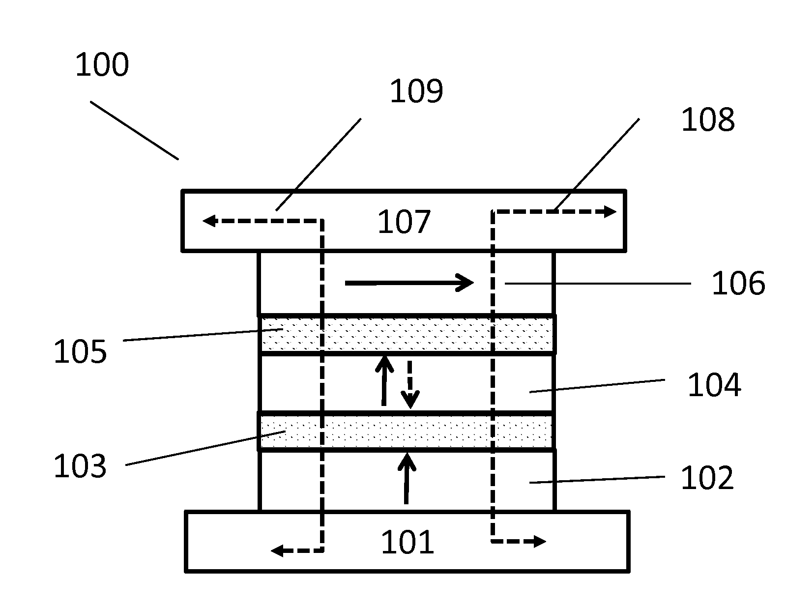
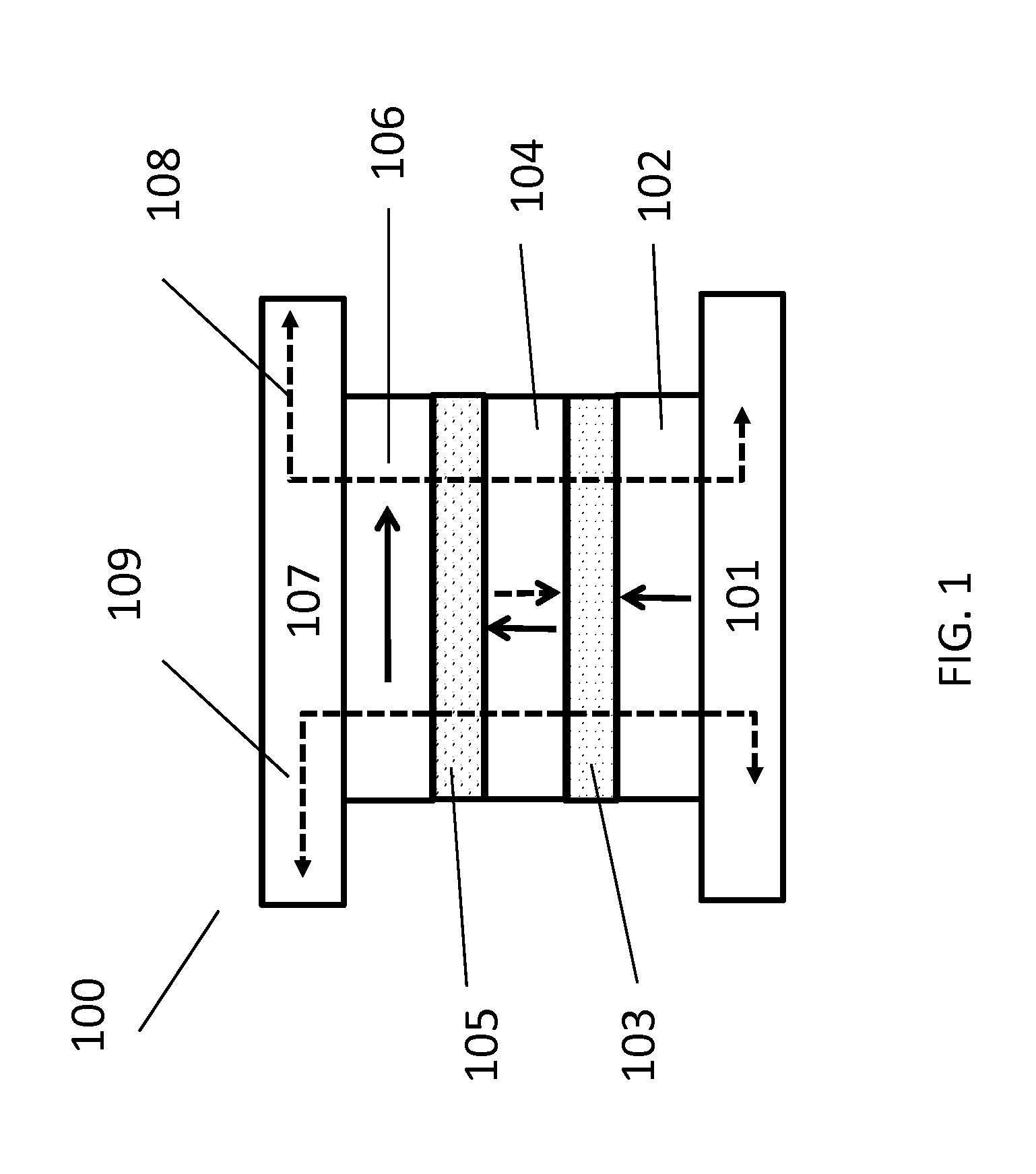
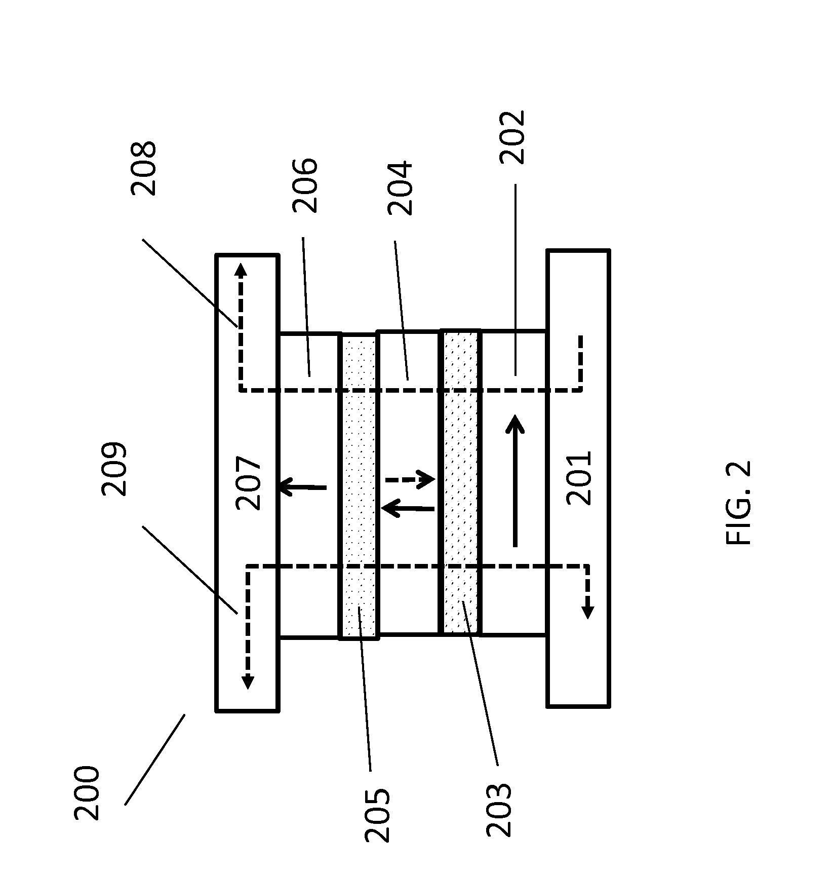
[0013]With reference of the FIG. 1 showing a magnetic memory cell 100, the proposed MRAM memory cell 100, counted from the material growth plane from the bottom, comprises a bottom electrode 101; perpendicular-anisotropy magnetic reference layer 102 with fixed magnetization orientation; tunneling barrier 103; perpendicular-anisotropy data storage layer 104; non-magnetic spacing layer 105; fi...


PUM


Abstract

A new magnetic memory cell comprises a perpendicular-anisotropy tunneling magnetic junction (TMJ) and a fixed in-plane spin-polarizing layer, which is separated from the perpendicular-anisotropy data storage layer of tunneling magnetic junction by a non-magnetic layer. The non-magnetic layer can be made of metallic or dielectric materials.

Description

FIELD OF INVENTION[0001]The invention is related to memory cell design for magnetoresistive random access memory (MRAM), more specifically design of a memory cell compromising perpendicular-anisotropy TMR sensing stack structure with perpendicular storage layer, whose magnetic orientation can be switched by spin polarization current injected from a fixed in-plane magnetic-anisotropy layer separated away by non-magnetic layer from storage layer.BACKGROUND ART[0002]Data storage memory is one of the backbones of the modern information technology. Semiconductor memory in the form of DRAM, SRAM and flash memory has dominated the digital world for the last forty years. Comparing to DRAM based on transistor and capacitor above the gate of the transistor, SRAM using the state of a flip-flop with large form factor is more expensive to produce but generally faster and less power consumption. Nevertheless, both DRAM and SRAM are volatile memory, which means they lost the information stored onc...

Claims


Application Information

Patent Timeline
Patent Type & Authority Applications(United States)
IPC IPC(8): H01L29/82
CPCG11C11/161H10N50/10
Inventor YI, GELI, SHAOPINGTANG, YUNJUNLIU, ZONGRONG
Owner GE YI
Why Eureka
Try Eureka