Method of forming an array of nanostructures

a nanostructure and array technology, applied in the field of nanofabrication methods, can solve the problems of high cost and low yield, and achieve the effects of high reliability, repeatability, and controllability, and inherent capability

Active Publication Date: 2013-11-14
THE BOARD OF TRUSTEES OF THE UNIV OF ILLINOIS
View PDF1 Cites 35 Cited by
  • Summary
  • Abstract
  • Description
  • Claims
  • Application Information

AI Technical Summary

Benefits of technology

[0123]Without involving any pre-patterning or nanoparticle assembly processes, this new nanomanufacturing method is highly reliable, repeatable, and controllable, as well as extremely time and cost effective as nanocone array structures on the entire wafer surface can be consistently created within a few minutes under room temperature. Considering all the above advantages over current antireflection coating processes, the inventors believe that this technology has an inherent capability to monolithically integrate with standard silicon device fabrication methods and can be readily adopted by today's silicon solar cell and high performance photonics industries.

Problems solved by technology

Since these approaches involve nanoscale pre-patterning, surface-area-sensitive assembly processes, or extreme fabrication conditions, they are often limited by high costs and low yields as well as by the consequent industry incompatibility.

Method used


Image

  • Method of forming an array of nanostructures
  • Method of forming an array of nanostructures
  • Method of forming an array of nanostructures

Examples


Embodiment Construction

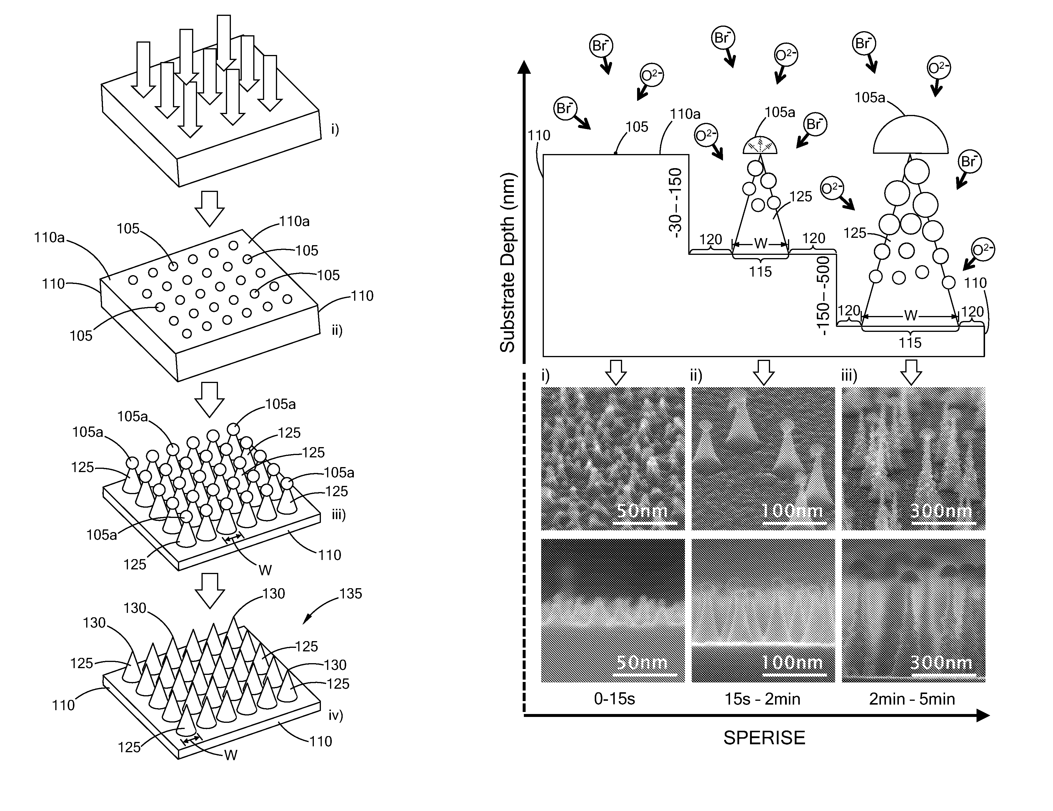
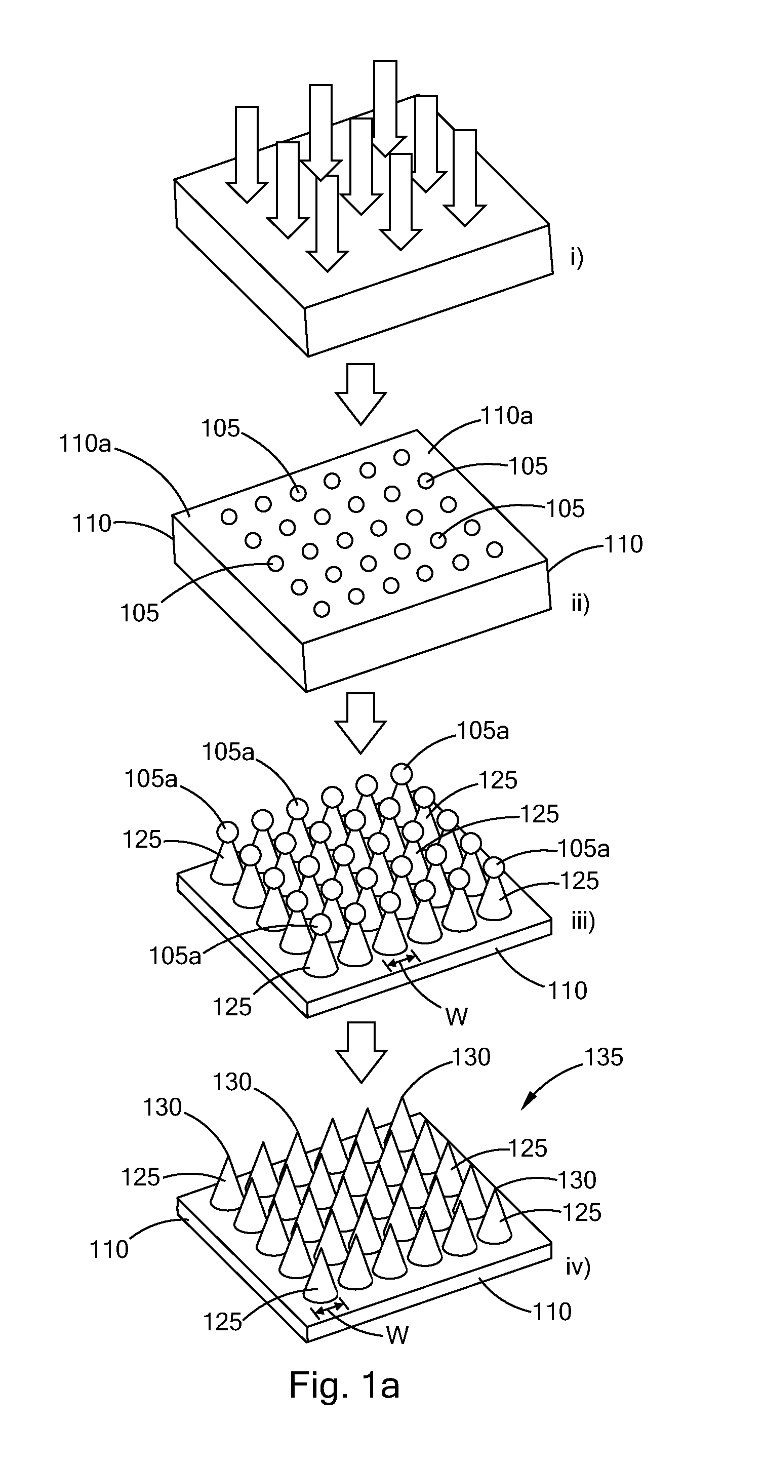
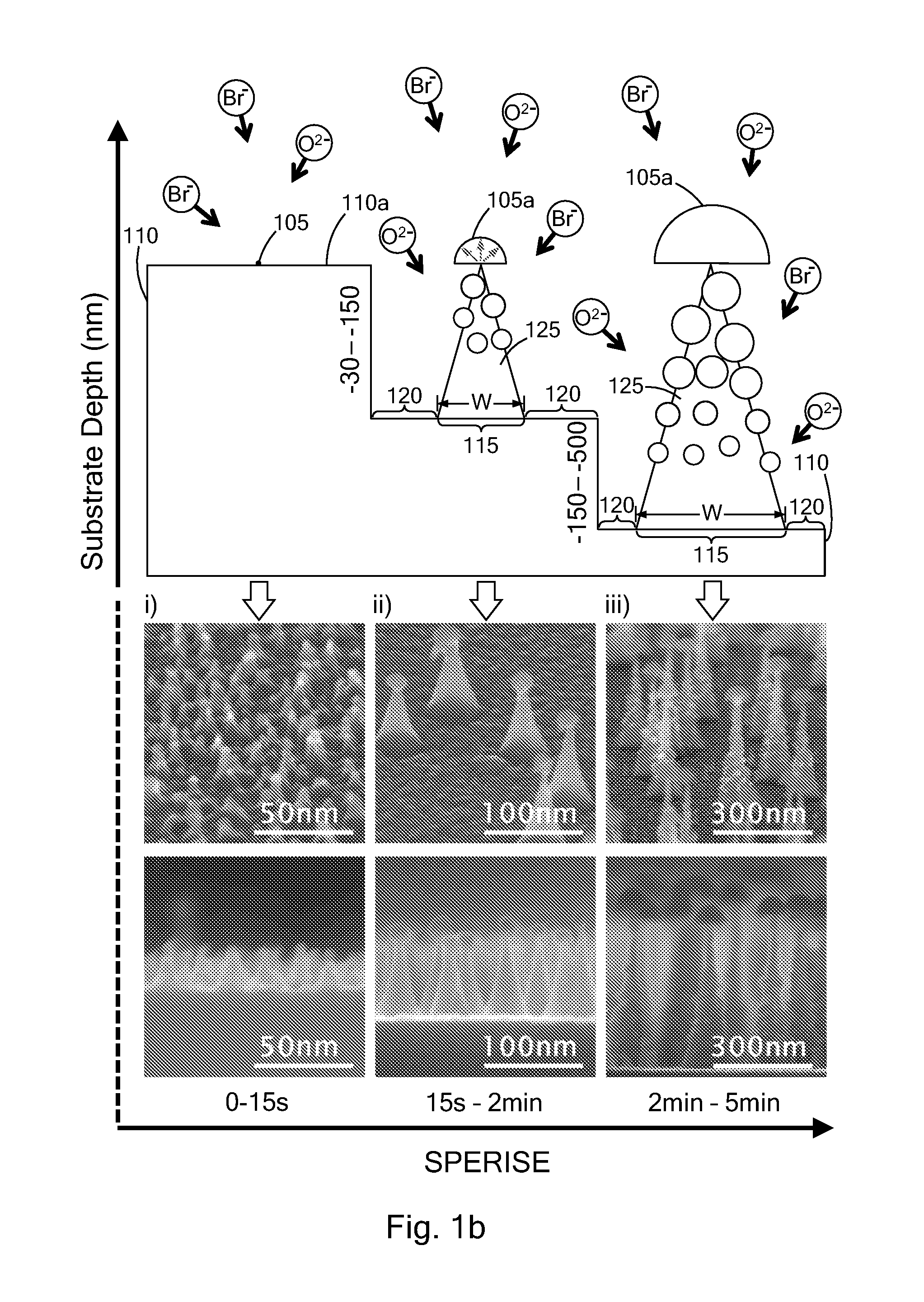
[0039]A unique, synchronized and simultaneous top-down and bottom-up nanofabrication approach called simultaneous plasma enhanced reactive ion synthesis and etching (SPERISE) is described. For the first time, the atomic addition and subtraction of nanomaterials can be concurrently observed and precisely controlled in a single step process permitting ultrahigh-throughput, lithography-less, wafer-scale and room-temperature nanomanufacturing. Rapid low-cost manufacturing of high-density, high-uniformity, light-trapping nanocone arrays has been demonstrated on single crystalline and polycrystalline silicon wafers, as well as on amorphous silicon thin films. Proposed nanofabrication mechanisms discussed below provide a general guideline to designing new SPERISE methods for other solid-state materials besides silicon.

[0040]A key mechanism underlying the SPERISE method is the concurrent reactive ion nucleation process with the reactive ion etching process. In a plasma-enhanced multiple ion...


PUM

PropertyMeasurementUnit
etch rateaaaaaaaaaa
etch rateaaaaaaaaaa
widthaaaaaaaaaa

Abstract

A method of forming an array of nanostructures includes forming a plurality of seed points on a surface of a substrate, and growing masks from the seed points to create masked regions of the substrate underlying the masks. A remainder of the substrate comprises an unmasked region. Each mask and masked region increase in size with growth time while the unmasked region of the substrate decreases in size. During the growing, the unmasked region is etched to remove material from the substrate in a depth direction, and, simultaneously, unetched structures are formed from the masked regions of the substrate underlying the masks. Each of the unetched structures has a lateral size that increases with depth.

Description

RELATED APPLICATIONS[0001]The present patent document claims the benefit of the filing date under 35 U.S.C. 119(e) of U.S. Provisional Patent Application Ser. No. 61,495,699, filed on Jun. 10, 2011, and U.S. Provisional Patent Application Ser. No. 61 / 408,945, filed on Nov. 1, 2010, both of which are hereby incorporated by reference in their entirety.FEDERALLY FUNDED RESEARCH OR DEVELOPMENT[0002]This invention was made with government support under contract number ECCS 10-28568 awarded by the National Science Foundation and under an Illinois ECE startup grant. The government has certain rights in this invention.TECHNICAL FIELD[0003]The present disclosure is related generally to a nanofabrication method and more particularly to a simultaneous plasma enhanced reactive ion synthesis and etching process.BACKGROUND[0004]The long-term industrial and societal impact of semiconductor nanofabrication technology depends on its production rate, reliability, robustness, yield, cost, and the inte...

Claims


Application Information

Patent Timeline
Patent Type & Authority Applications(United States)
IPC IPC(8): H01L21/02H01L31/0352H01L29/06
CPCH01L21/02612H01L29/0665H01L31/035209B82Y30/00B82Y40/00H01L31/02363H01L31/035227H01L31/1804Y02E10/547B82Y20/00Y02P70/50
Inventor CHEN, YILIU, G. LOGAN
Owner THE BOARD OF TRUSTEES OF THE UNIV OF ILLINOIS
Why Eureka
Try Eureka