Line and space architecture for a non-volatile memory device

Inactive Publication Date: 2013-11-14
CROSSBAR INC
View PDF2 Cites 0 Cited by
  • Summary
  • Abstract
  • Description
  • Claims
  • Application Information

AI Technical Summary

Benefits of technology

[0008]In various embodiments, resistive random accessed memory device (commonly known as RRAM or ReRAM) configured in a crossbar array has an unique advantage of forming a high density memory device. Each of the RRAM comprises of a top electrode, a bottom electrode, and a resistive switching material formed in between the first electrode and the second electrode. The resistive switching material is characterized by a resistance depending on an electric field applied to the electrodes. For a small feature size, the resistive switching element pre

Problems solved by technology

Lithography to print such a small feature for etching is difficult and usually results in defects and yield loss.
Additionally, RRAM device may use non-conventional materials not normally used in CMOS process and may complicate the CMOS fabrication process.

Method used


Image

  • Line and space architecture for a non-volatile memory device
  • Line and space architecture for a non-volatile memory device
  • Line and space architecture for a non-volatile memory device

Examples


Example

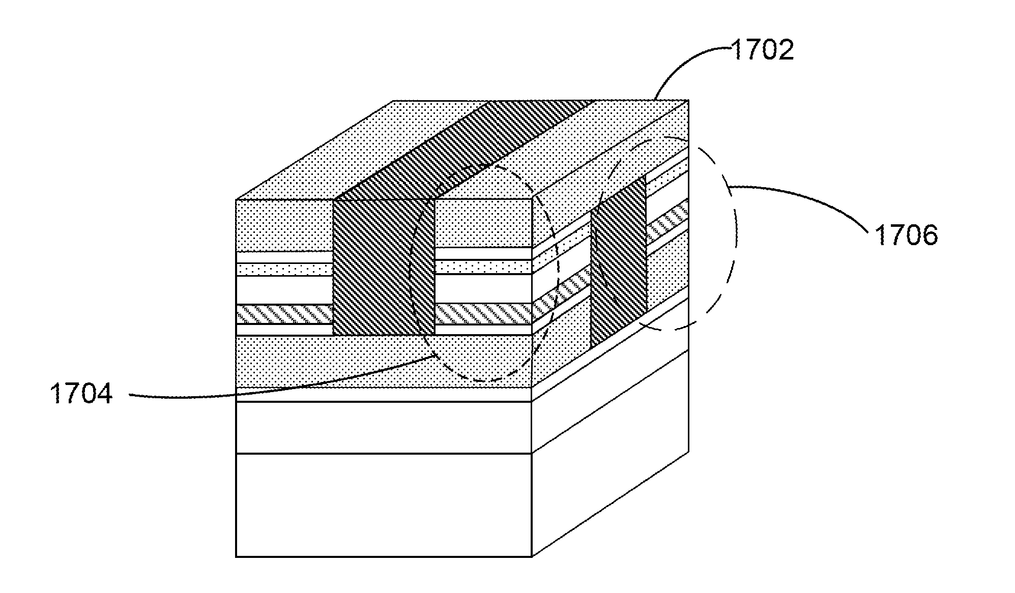
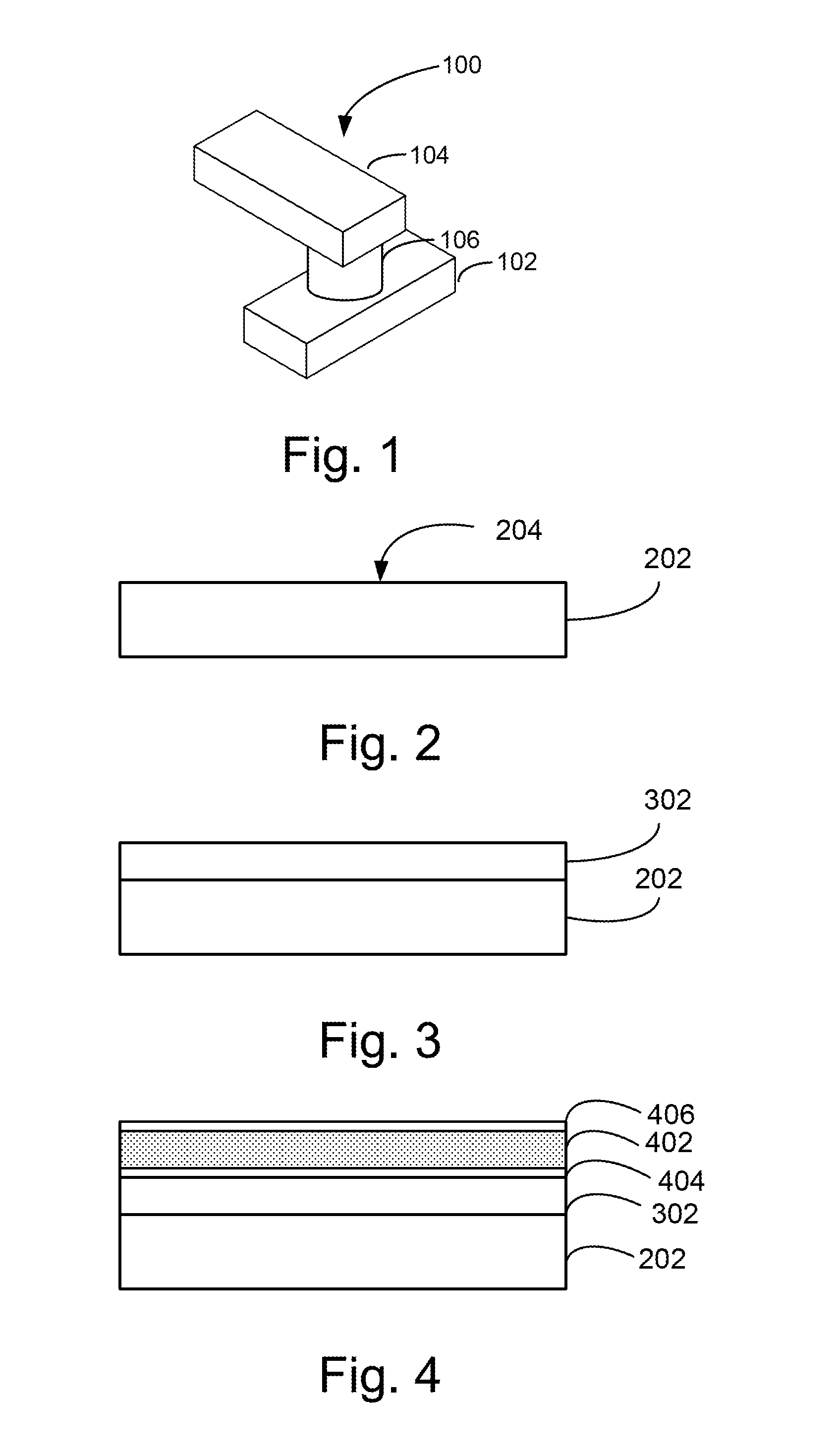
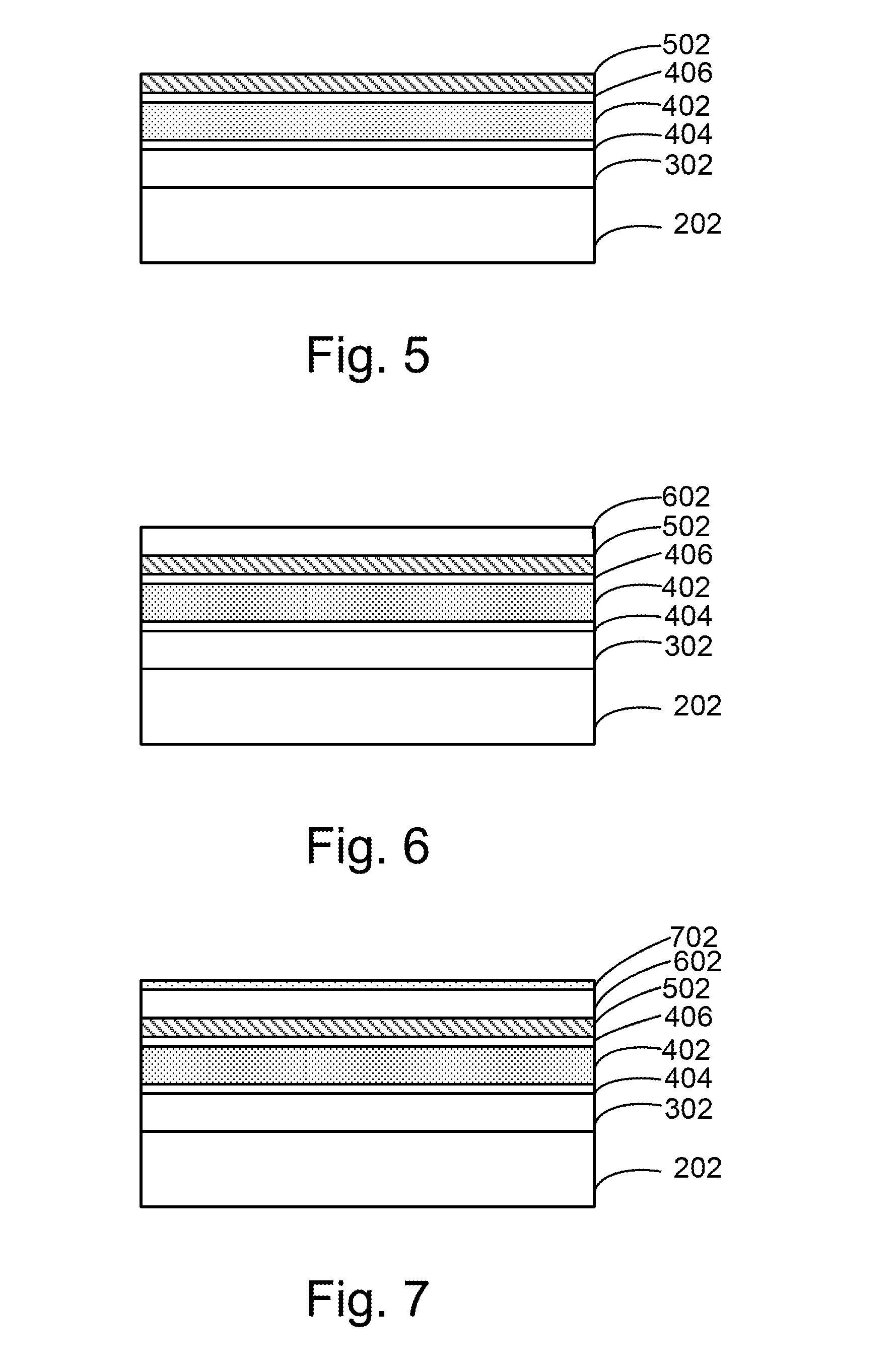
[0033]The present invention is generally related to resistive switching devices. More particularly, embodiments according to the present invention provide a method and a structure to form a resistive switching device. Embodiments according to the present invention can be applied to non-volatile memory devices but it should be recognized that the present invention can have a much broader range of applicability.

[0034]FIG. 1 is a simplified diagram of a resistive switching device 100. As shown, resistive switching device 100 includes a first electrode 102, a second electrode 104 and a resistive switching element 106 configured in an intersection region between the first electrode and the second electrode. First electrode 102 can be a metal material or a doped semiconductor material used in conventional CMOS processing. For example, the first electrode can be copper, tungsten, aluminum, or a doped semiconductor material.

[0035]Resistive switching element can be a suitable insulator mater...


PUM


Abstract

A non-volatile memory device includes first wiring structures elongated in a first direction and separated by a first gap region in a second direction, the first gap region comprising first dielectric material formed in a first process, second wiring structures elongated in a second direction and separated by a second gap region in a first direction, the second gap region comprising second dielectric material formed in a second process, and a resistive switching devices comprising active conductive material, resistive switching material, and a junction material, wherein resistive switching devices are formed at intersections of the first wiring structures and the second wiring structures, wherein the junction material comprising p+ polysilicon material overlying the first wiring material, wherein some resistive switching devices are separated by the first gap region and some resistive switching devices separated by the second gap region.

Description

BACKGROUND[0001]The present invention is generally related to resistive switching devices. More particularly, embodiments according to the present invention provide a method and a structure to form a resistive switching device. Embodiments according to the present invention can be applied to non-volatile memory devices but it should be recognized that the present invention can have a much broader range of applicability.[0002]The inventor of the present invention has recognized the success of semiconductor devices has been mainly driven by an intensive transistor down-scaling process. However, as field effect transistors (FETs) approach sizes less than 100 nm, physical problems such as short channel effect begin to hinder proper device operation. For transistor based memories, such as those commonly known as Flash memories, other performance degradations or problems may occur as device sizes shrink. With Flash memories, a high voltage is usually required for programming of such memor...

Claims


Application Information

Patent Timeline
IPC IPC(8): H01L27/26H01L47/00
CPCH01L45/085H01L45/1233H01L45/1675H01L45/1616H01L45/148H10N70/245H10N70/826H10N70/884H10N70/023H10N70/063
Inventor MAXWELL, STEVEN PATRICK
Owner CROSSBAR INC
Why Eureka
Try Eureka