Temporary adhesive for wafer processing, member for wafer processing using the same, wafer processed body, and method for producing thin wafer
a technology of temporary adhesives and wafers, applied in the direction of heat-activated film/foil adhesives, film/foil adhesives, synthetic resin layered products, etc., can solve the problems of inability to meet the requirements of tsv formation process and back surface wiring layer formation process, inability to use expensive laser equipment, etc., to achieve the effect of easy production, easy separation and easy handling
- Summary
- Abstract
- Description
- Claims
- Application Information
AI Technical Summary
Benefits of technology
Problems solved by technology
Method used
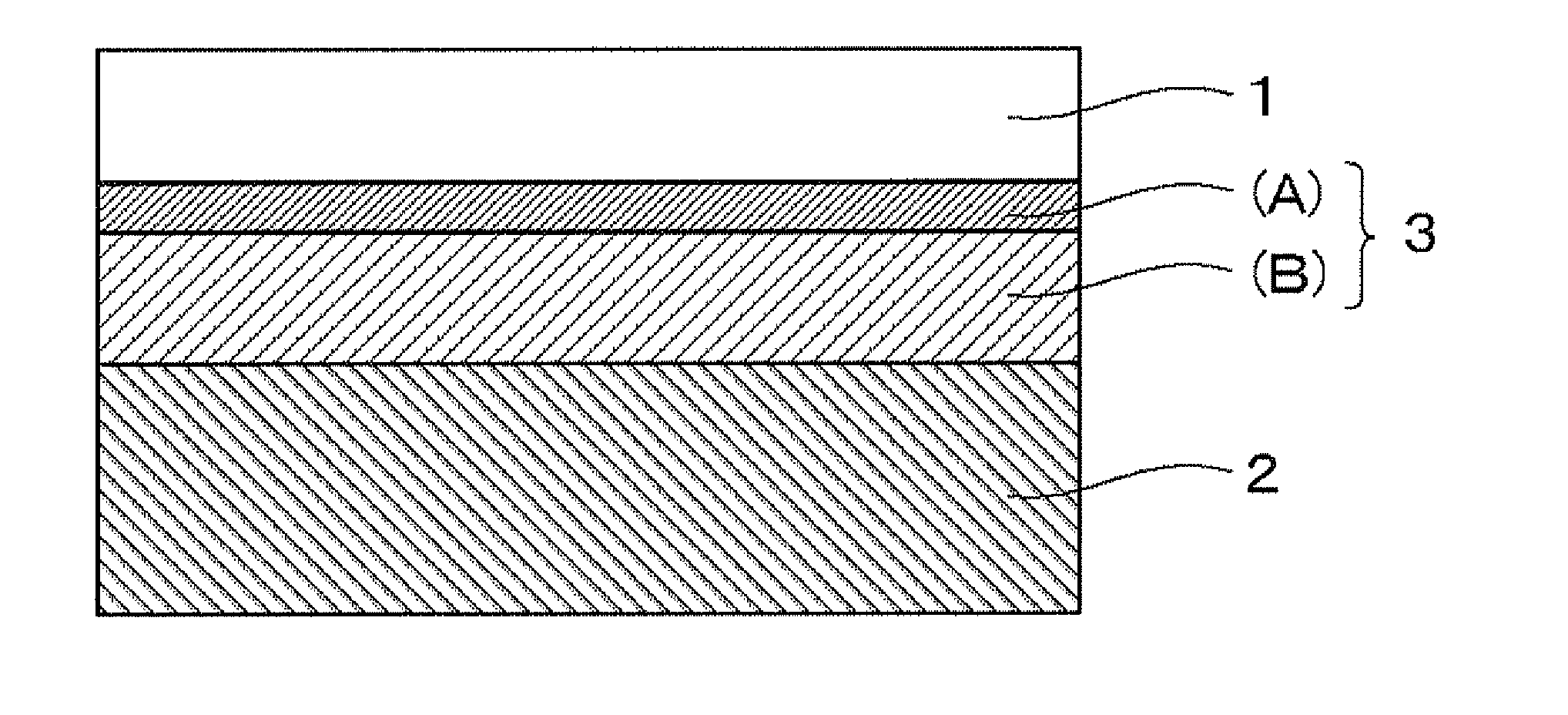
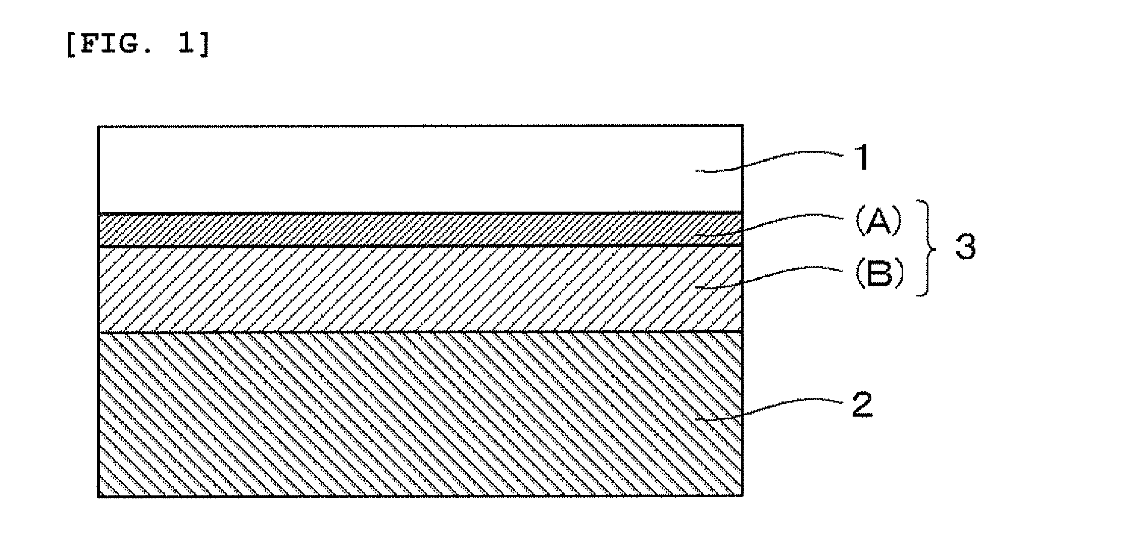
Image

Examples
synthesis example 1
Resin Synthesis Example 1
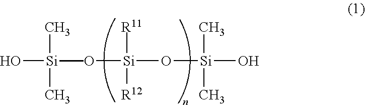
[0089]80 parts of dimethyl polysiloxane (in the general formula (1), n was 9,000) which was a raw rubber having both terminals of molecular chain blocked with hydroxyl groups and had a viscosity at 25° C. in 30% toluene solution of 98,000 mPa·s, and 20 parts of methylpolysiloxane resin which had a molar ratio of (CH3)SiO1 / 2 unit to SiO4 / 2 unit of 0.75 to 1 and had 1.0% by mole hydroxyl group relative to 100 of solid content were taken into a four-necked flask and dissolved in 900 parts of toluene. To the resulting solution, 1 part of 28% ammonia water was added, and the mixture was stirred at room temperature for 24 hours to cause a condensation reaction. The resultant was heated at 180° C. under reduced pressure to remove toluene, condensed water, and ammonia. As a result, a partial condensate which had been solidified was obtained.
[0090]900 parts of toluene was added to 100 parts of the resulting partial condensate and dissolved. To the resulting solution,...
synthesis example 2
Resin Synthesis Example 2
[0093]90 parts of dimethyl polysiloxane (in the general formula (1), n was 9,000) which was a raw rubber having both terminals of molecular chain blocked with hydroxyl groups and had a viscosity at 25° C. in 30% toluene solution of 98,000 mPa·s, and 10 parts of methylpolysiloxane resin which had a molar ratio of (CH3)SiO1 / 2 unit to SiO1 / 2 unit of 0.75 to 1 and had 1.0% by mole hydroxyl group relative to 100 of solid content were taken into a four-necked flask and dissolved in 900 parts of toluene. To the resulting solution, 1 part of 28% ammonia water was added, and the mixture was stirred at room temperature for 24 hours to cause a condensation reaction. The resultant was heated at 180° C. under reduced pressure to remove toluene, condensed water, and ammonia. As a result, a partial condensate which had been solidified was obtained. 900 parts of toluene was added to 100 parts of the partial condensate and dissolved. To the resulting solution, 20 parts of he...
synthesis example 3
Resin Synthesis Example 3
[0095]95 parts of dimethyl polysiloxane (in the general formula (1), n was 9,000) which was a raw rubber having both terminals of molecular chain blocked with hydroxyl groups and had a viscosity at 25° C. in 30% toluene solution of 98,000 mPa·s, and 5 parts of methylpolysiloxane resin which had a molar ratio of (CH3)SiO1 / 2 unit to SiO4 / 2 unit of 0.75 to 1 and had 1.0% by mole hydroxyl group relative to 100 of solid content were taken into a four-necked flask and dissolved in 900 parts of toluene. To the resulting solution, 1 part of 28% ammonia water was added, and the mixture was stirred at room temperature for 24 hours to cause a condensation reaction. The resultant was heated at 180° C. under reduced pressure to remove toluene, condensed water, and ammonia. As a result, a partial condensate which had been solidified was obtained. 900 parts of toluene was added to 100 parts of the partial condensate and dissolved. To the resulting solution, 20 parts of hex...
PUM
| Property | Measurement | Unit |
|---|---|---|
| molar ratio | aaaaa | aaaaa |
| molar ratio | aaaaa | aaaaa |
| temperature | aaaaa | aaaaa |
Abstract
Description
Claims
Application Information
PatSnap Eureka turns technology decisions into work you can execute. Powered by our Innovation Knowledge Graph, it runs expert workflows across engineering, life sciences, materials and intellectual property. Get your review-ready output in minutes.


