Td converter and ad converter with no operational amplifier and no switched capacitor

a technology of ad converter and switched capacitor, which is applied in the direction of code conversion, transmission system, instruments, etc., can solve the problems of linearity degradation, scale shrinkage becomes difficult, dynamic range narrowing, etc., and achieves the effect of propagated quantization error, small area, and high linearity

Inactive Publication Date: 2013-11-21
SEMICON TECH ACADEMIC RES CENT
View PDF4 Cites 19 Cited by
  • Summary
  • Abstract
  • Description
  • Claims
  • Application Information

AI Technical Summary

Benefits of technology

[0020]In view of the aforementioned circumstances, the present invention has a first object to provide a high-resolution operational-amplifier-less capacitor-less TD converter, whose switching noises are reduced by reducing the amount of currents that change at the time of the gating operation of the oscillator.
[0021]A second object of the present invention is to provide a high-resolution operational-amplifier-less capacitor-less TD converter, which scarcely receives the influences of leakage currents by obviating the need for statically retaining the phase information by means of stopping the oscillator.
[0022]A third object of the present invention is to provide an operational-amplifier-less capacitor-less higher-order TD converter, which can perform higher-order noise shaping by propagating the quantization error by improving the linearity of the circuit that propagates the quantization error.

Problems solved by technology

However, the scale shrinkage becomes difficult due to dynamic range and the problem of nonlinearity in the analog circuits such as operational amplifiers and switched capacitors.
In particular, under environments of low power voltages in the advanced processes, the dynamic range narrows and the linearity deteriorates, and this leads to difficulties in securing gain.
In the above circuit configuration, the gating operation (turning on and off of Tin and TQN1) of the GRO 11 adversely affects the internal phase information as switching noises.
Since the leakage currents tend to increase as the process scale shrinkage advances, the above circuit configuration is unsuitable for scale shrinkage.
These problems become obstructions in increasing the resolutions of the TD converter and the AD converter.

Method used


Image

  • Td converter and ad converter with no operational amplifier and no switched capacitor
  • Td converter and ad converter with no operational amplifier and no switched capacitor
  • Td converter and ad converter with no operational amplifier and no switched capacitor

Examples


first preferred embodiment

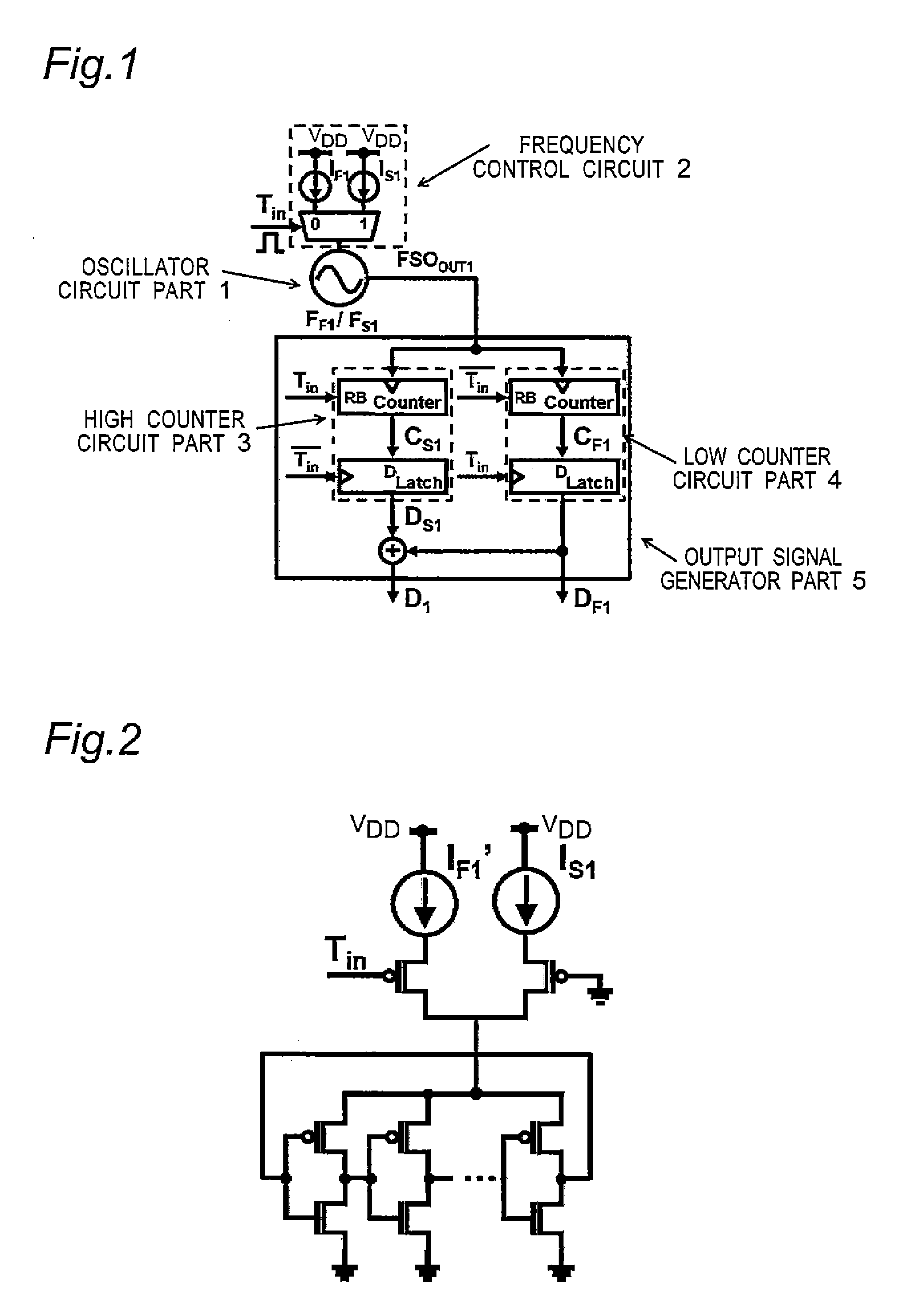
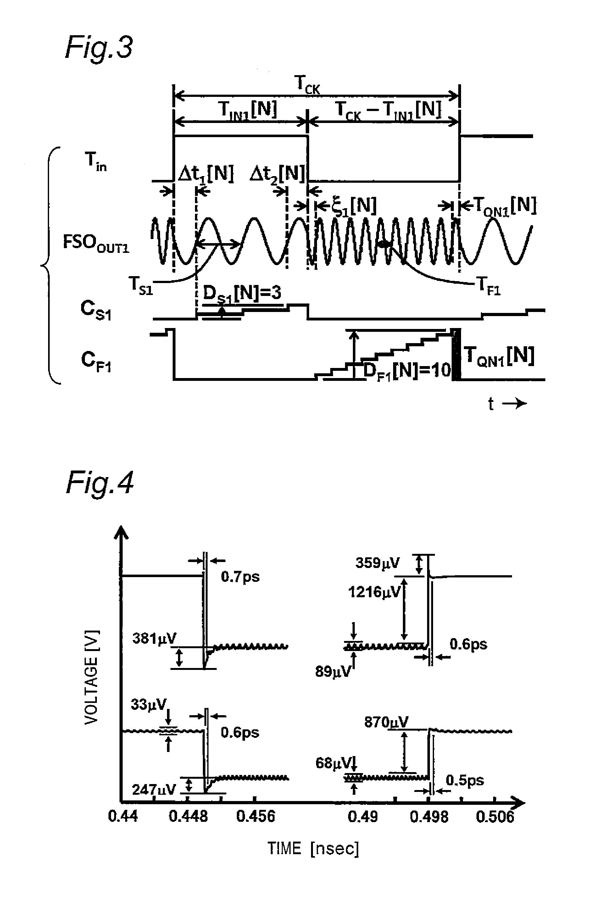
[0070]FIG. 1 shows a circuit configuration diagram of the first-order TD converter of the first preferred embodiment.

[0071]The first-order TD converter of the first preferred embodiment is configured to include: a one-stage oscillator circuit part configured to input time domain data (Tin); a High counter circuit part that includes a High counter configured to measure the number of waves of the output oscillation waveform from the oscillator circuit part when the time domain data is “High” and a High register configured to store the number of waves when the time domain data is “High” at the preceding sampling; a Low counter circuit part that includes a Low counter configured to measure the number of waves of the output oscillation waveform of the oscillator circuit part when the time domain data is “Low” and a Low register configured to store the number of waves when the time domain data is “Low” at the preceding sampling; an adder configured to add a High register value to a Low re...

second preferred embodiment

[0085]FIG. 5 shows a circuit configuration diagram of a second-order TD converter of the second preferred embodiment.

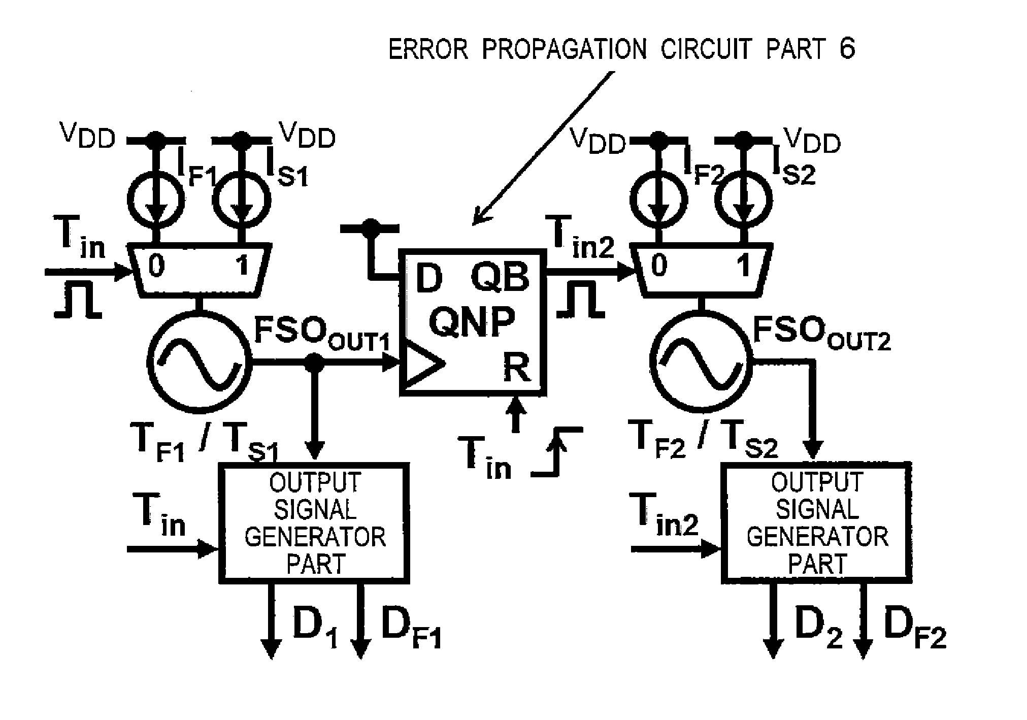
[0086]The second-order TD converter of the second preferred embodiment is configured to include: a two-stage oscillator circuit part configured to input time domain data (Tin and Tin2); an error propagation circuit part that is inserted between the oscillator circuit part of the preceding stage and the oscillator circuit part of the succeeding stage, takes out delay information including quantization error from the phase information of the oscillator circuit part of the preceding stage, and propagates the information as time domain data (Tin2) of the succeeding stage to the oscillator circuit part of the succeeding stage; a High counter circuit part that includes a High counter configured to measure the number of waves of the output oscillation waveform of the oscillator circuit part when the time domain data of each stage is “High” and a High register configured to s...

third preferred embodiment

[0102]FIG. 11 shows a circuit configuration diagram where the second-order TD converter of the second preferred embodiment is extended to the third-order TD converter of the third preferred embodiment.

[0103]FIG. 12 is a schematic chart of the waveforms of the oscillator circuit when the third-order TD converter operates. A digital output DOUT3 of which the quantization error has undergone third-order noise-shaping can be obtained as the following Equations (15) and (16) by estimating W2=−A3 / B2 in a manner similar to that of the second preferred embodiment except for the symbol “i”=1, 2, 3. It is also possible to extend it to a higher order. In the following Equations (15) and (16), C8 and C9 are constants:

D3′=D3-w2DF2=-A3TQN2-B3(1-z-1)TQN3+C8,and(15)DOUT3=-w2DOUT2+D3′(1-z-1)2=A1w1w2TIN1-B3(1-z-1)3TQN3+C9.(16)


PUM


Abstract

A TD converter is provided for digitally converting a delay time value into a digital value. In the TD converter, an oscillator circuit part inputs time domain data. A first-state counter circuit part measures a number of waves of an output oscillation waveform from the oscillator circuit part when time domain data is in a first state, and a second-state counter circuit part measures a number of waves of the output oscillation waveform from the oscillator circuit part when the time domain data is in a second state. An output signal generator part generates an output signal based on output count values of the first-state counter circuit part and the second-state counter circuit part, and a frequency control circuit controls the oscillator circuit part to always oscillate and to control an oscillation frequency of the oscillator circuit part.

Description

BACKGROUND OF THE INVENTION[0001]1. Field of the Invention[0002]The present invention relates to a TD (Time to Digital) converter that uses calculation in a time domain instead of using neither operational amplifier nor switched capacitor regarded as unsuitable for process scale shrinkage.[0003]2. Description of the Related Art[0004]It is indispensable to develop an LSI that has lower power consumption, higher performance and lower cost than conventional ones for further development of information communication equipment. The performances of conventional LSIs have been improved in accordance with the scale shrinkage of semiconductor manufacturing processes. The mounted transistor count per chip increases every year by virtue of scale shrinkage, and this allows higher performance LSIs to be actualized.[0005]However, the scale shrinkage becomes difficult due to dynamic range and the problem of nonlinearity in the analog circuits such as operational amplifiers and switched capacitors. ...

Claims


Application Information

Patent Timeline
Patent Type & Authority Applications(United States)
IPC IPC(8): H03M1/50
CPCH03M1/50G04F10/005
Inventor KAWAGUCHI, HIROSHIYOSHIMOTO, MASAHIKOKONISHI, TOSHIHIROIZUMI, SHINTAROOKUNO, KEISUKE
Owner SEMICON TECH ACADEMIC RES CENT
Why Eureka
Try Eureka