
Image processing device and computer program for performing image processing

a technology of image processing and computer program, which is applied in the direction of semiconductor/solid-state device testing/measurement, instruments, photomechanical equipment, etc., can solve the problem of difficulty in making coincidence-degree judgment with a high accuracy, and achieve the effect of convenient implementation

Inactive Publication Date: 2013-12-05
HITACHI HIGH-TECH CORP
View PDF11 Cites 23 Cited by
  • Summary
  • Abstract
  • Description
  • Claims
  • Application Information

AI Technical Summary

Benefits of technology

The patent text describes a way to create an image that is similar to an image captured using a charged-particle beam device. This is useful for creating templates for matching and verifying the device's output. The technique makes it easy to create the necessary templates without using the device itself.

Problems solved by technology

As a result, in some cases, it becomes difficult to make the coincidence-degree judgment with a high accuracy.

Method used


Image

  • Image processing device and computer program for performing image processing
  • Image processing device and computer program for performing image processing
  • Image processing device and computer program for performing image processing

Examples


embodiment 1

[0046]As described earlier, the automated operation of the measurement in the semiconductor fabrication processes occupies an important role in the efficient implementation of the entire production steps. On account of the factors that will be pointed out hereinafter, however, the measurement-recipe-based automated operation of the measurement has become an obstruction to the implementation of an enhancement in the automated ratio.

[0047]In the semiconductor fabrication, the pattern shape is formed on a silicon wafer by a light-exposure device, using a mask-reticle that is created based on pre design data in order to transfer the corresponding target pattern. Also, in etching steps, a desired pattern is formed by removing unnecessary portions by the etching on the target pattern.

[0048]In the wafer pattern formation, a variety of variation factors in the above-described semiconductor fabrication steps result in a variation in the pattern dimension that becomes the measurement target. ...

embodiment 2

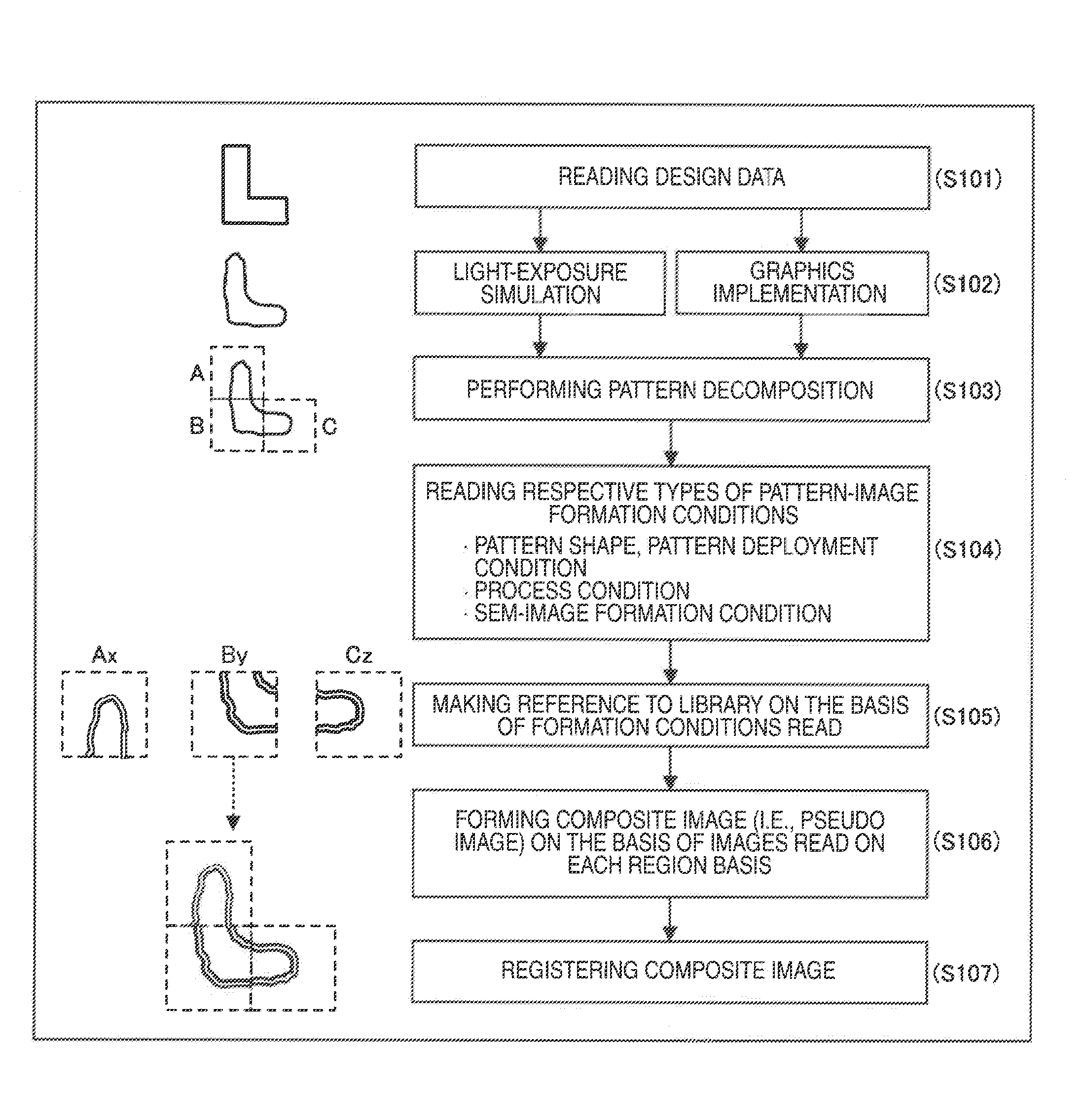
[0065]Next, the explanation will be given below concerning an example where the pseudo image is formed not by registering the images, but by performing an image processing. FIG. 9 is a diagram for illustrating steps through which the pseudo image is formed based on this image processing. FIG. 10 is a flowchart for these steps. First, the layout data is read from the design-data storage medium 218 (step S1001). Next, the light-exposure simulation is carried out using the simulator 220 (step S1002). Moreover, a simulation image, which is obtained by the simulation, is decomposed in the layout-data decomposition unit 212. After that, luminance-distribution information and luminance-value information are extracted from the library, depending on the attribute information on each decomposed area (step S1003). Incidentally, in the present embodiment, the explanation will be given regarding only the pattern region A (i.e., one of the decomposed areas).

[0066]FIG. 6 is a diagram for illustrat...

embodiment 3

[0069]The explanation given so far has related to the case where the composite image (i.e., pseudo image) is registered as the template. In the following explanation, however, the explanation will be given regarding the following case: Namely, the pseudo image is used as a verification image for the verification of an already-existing template, or a newly-created template. In other words, the present explanation relates to a device or the like for performing the verification or the like of validity of a measurement recipe. Here, the measurement recipe is used when measuring semiconductor-light-exposure-used mask shape, and silicon shape, i.e., exposed semiconductor-transferred pattern, in the semiconductor fabrication processes. The verification like this, and the verification-based correction of the measurement recipe are performed properly. These operations allow implementation of an enhancement in the production efficiency in the semiconductor fabrication processes.

[0070]In the p...


PUM


Abstract

It is an object of the present invention to provide an image processing device for allowing an actual-image-closer pattern to be formed based on the design data, or its simulation image. In order to accomplish the above-described object, the proposal is made concerning an image processing device which includes an image processing unit which sets the operation condition of a charged-particle beam device on the basis of the design data on a semiconductor element. Here, the image processing device accesses a library for storing device-condition information on the charged-particle beam device, pattern types, and a plurality of combinations of pattern information on each pattern-region basis. Moreover, the image processing device forms a composite image of each pattern region, using the pattern information on each pattern-region basis, and based on the device-condition information and the selection of a pattern type from the pattern types.

Description

TECHNICAL FIELD[0001]The present invention relates to an image processing device and charged-particle beam device for performing the dimension measurement and inspection of a pattern formed on a sample. More specifically, it relates to an image processing device and computer program for allowing setting of the measurement and inspection condition for a measurement device or inspection device.BACKGROUND ART[0002]In a device for measuring and inspecting a pattern formed on a semiconductor wafer, the template-matching technology is used in order to focus the microscope's field-of-view (: FOV) onto a desired measurement position. The template-matching technology is an image processing technology for finding out from inside a to-be-searched image, an area that coincides most with a template image registered in advance. The template-matching technology is known as a technique that is effective for searching for a microminiaturized pattern. The template-matching-used template image needs t...

Claims


Application Information

Patent Timeline
IPC IPC(8): G06F17/50
CPCG06F17/50G01B15/04H01L22/12G03F7/70625H01L2924/0002H01L2924/00G06F30/00
Inventor MATSUOKA, RYOICHIMITO, HIROAKI
Owner HITACHI HIGH-TECH CORP
Learn More