Chip-component structure

a chip and component technology, applied in the field of chip component structure, can solve the problems of acoustic noise likely to be produced by the circuit board, and the circuit board produces acoustic noise, so as to prevent the production of acoustic noise in the circuit board, reduce the amount of joining material, and small the line width of the side electrod

Active Publication Date: 2013-12-12
MURATA MFG CO LTD
View PDF10 Cites 33 Cited by
  • Summary
  • Abstract
  • Description
  • Claims
  • Application Information

AI Technical Summary

Benefits of technology

[0025]In this structure, the component connecting electrode and the external connection electrode are connected using the in-hole electrode provided in the through-hole of the interposer. Thus, a current path is ensured by the in-hole electrode and ESL is significantly reduced even when the line width of the side electrode is small. Further, since the line width of the side electrode is small, it is possible to reduce the amount of joining material that wets and spreads on the side electrode and to significantly reduce and prevent production of acoustic noise in the circuit board.
[0026]By using the chip-component structure according to the various preferred embodiments of the present invention, the amount of solder that reaches the outer electrode of the multilayer capacitor is significantly reduced and production of audible noise in the circuit board is significantly reduced and prevented. Further, magnetic fields produced in the interposer by the in-hole electrodes cancel each other, and current paths are dispersed by addition of the side lines. This reduces the inductances of the in-hole electrodes and the side lines, and greatly reduces ESL.

Problems solved by technology

When the distortions are transmitted to the circuit board, acoustic noise is produced by the circuit board.
Consequently, distortion of the capacitor is likely to be transmitted to the circuit board via the joining material such that acoustic noise is likely to be produced from the circuit board.

Method used


Image

  • Chip-component structure
  • Chip-component structure
  • Chip-component structure

Examples


first preferred embodiment

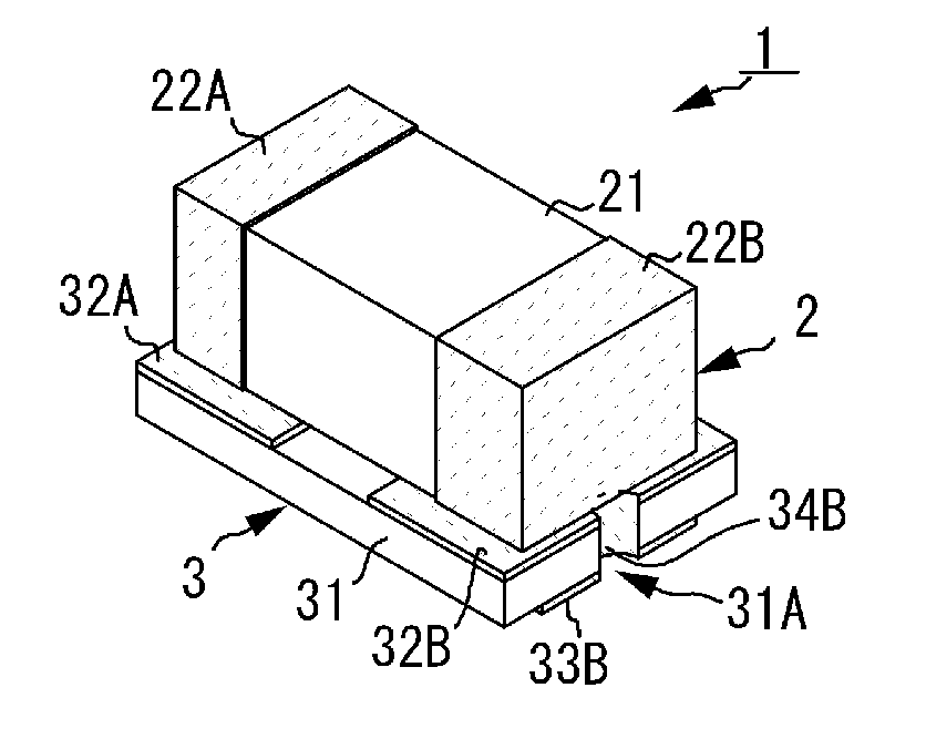
[0039]A chip-component structure 1 according to a first preferred embodiment of the present invention will be described below.

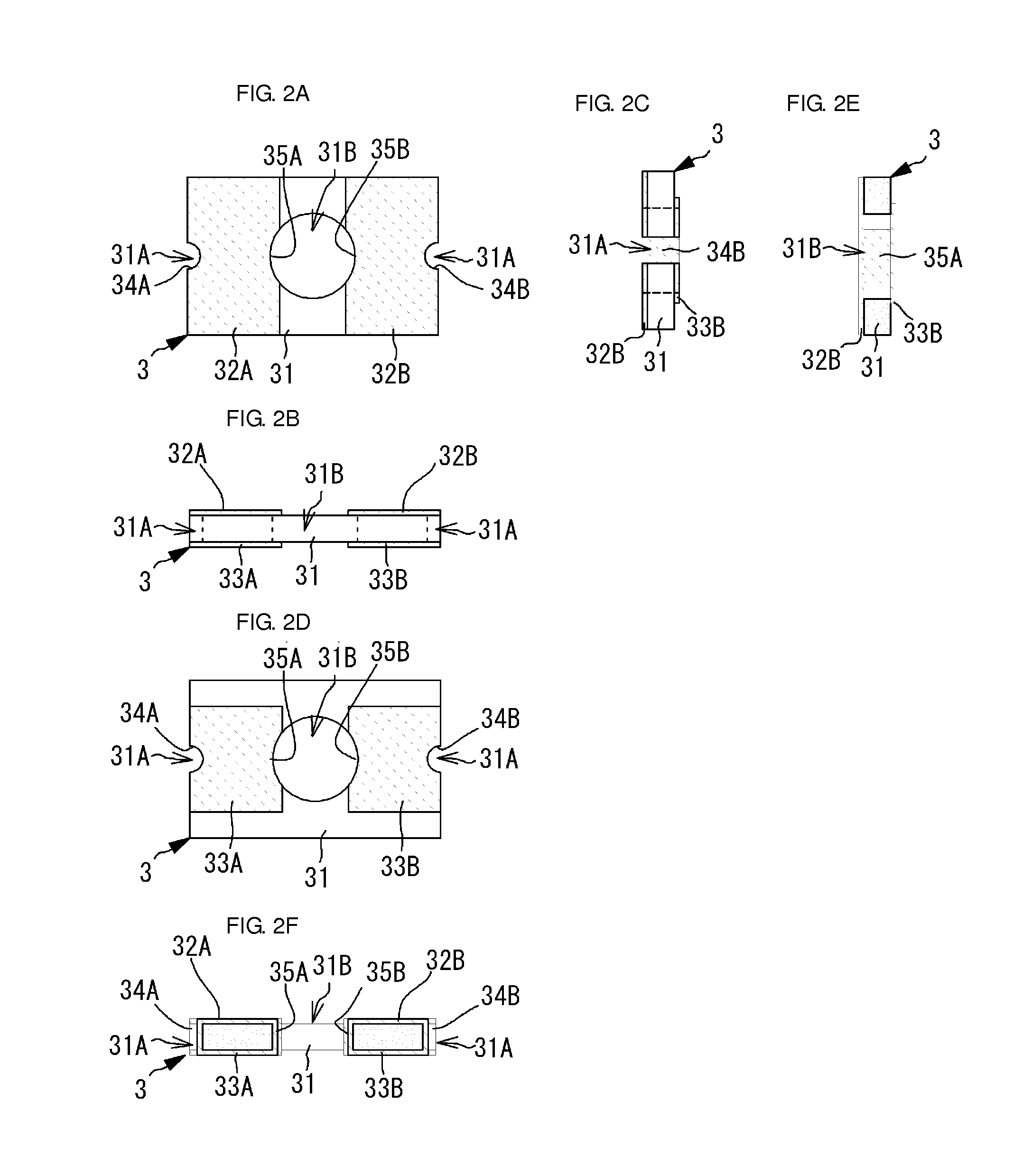
[0040]The chip-component structure 1 preferably includes a multilayer capacitor 2 and an interposer 3. Detailed structures of the multilayer capacitor 2 and the interposer 3 will be described below.

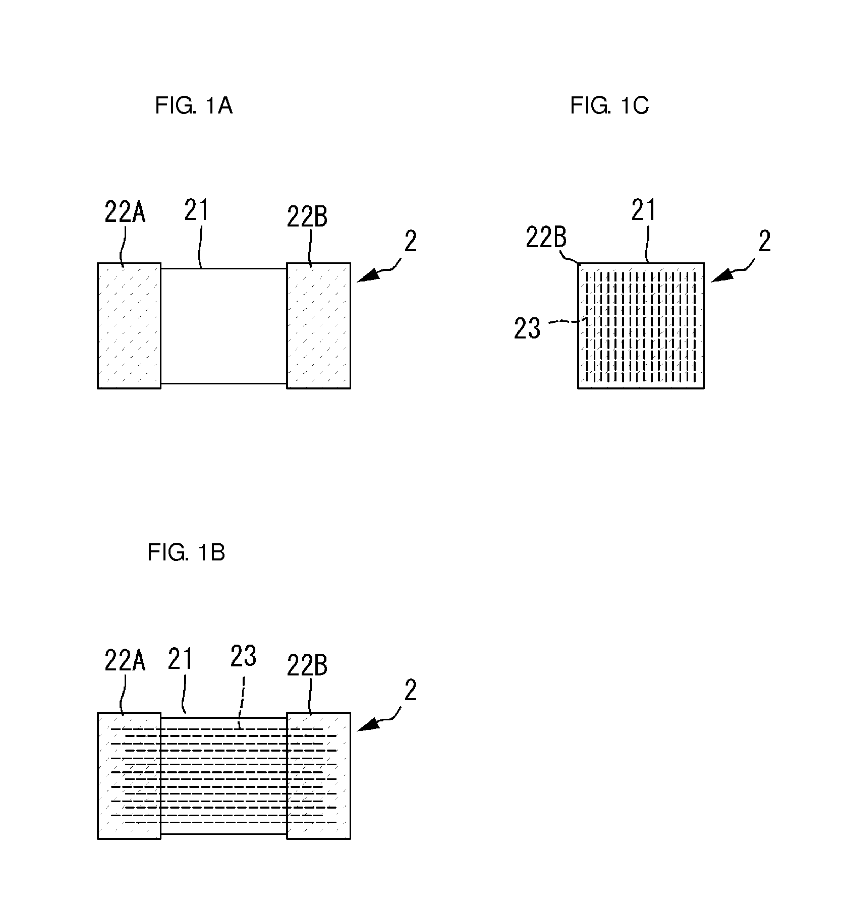
[0041]FIGS. 1A, 1B, and 1C are a plan view, a front view, and a right side view, respectively, of the capacitor 2.

[0042]The capacitor 2 preferably includes a laminated body 21, outer electrodes 22A and 22B, and inner electrodes 23. The laminated body 21 preferably is shaped like a rectangular or substantially rectangular parallelepiped including both longitudinal end surfaces (right and left side surfaces in FIGS. 1A to 1C) of a square or substantially square shape, and is defined by a plurality of dielectric layers stacked in a lateral direction. Also, in the laminated body 21, the inner electrodes 23 are stacked with the dielectric layers being disposed therebetw...

second preferred embodiment

[0075]FIGS. 7A, 7B, and 7C are a plan view, a sectional front view, and a bottom view, respectively, of a chip-component structure 1A according to a second preferred embodiment of the present invention.

[0076]The chip-component structure 1A of the second preferred embodiment is preferably the same or substantially the same in the structure of a multilayer capacitor 2 as the chip-component structure 1 of the first preferred embodiment, but is different in that an interposer 3A having a different size is provided. For this reason, in the following description, structures corresponding to the structures adopted in the first preferred embodiment are denoted by the same reference numerals.

[0077]The outer shape of the interposer 3A in plan view is preferably identical or substantially identical to that of the multilayer capacitor 2. For this reason, arcs of grooves 31A provided in both longitudinal end surfaces of a substrate body 31 are entirely located under bottom surfaces of outer elec...

third preferred embodiment

[0080]FIGS. 8A, 8B, and 8C are a plan view, a sectional front view, and a bottom view, respectively, of a chip-component structure 1B according to a third preferred embodiment of the present invention.

[0081]The chip-component structure 1B of the third preferred embodiment is preferably the same in the structure of a multilayer capacitor 2 as the chip-component structure 1 of the first preferred embodiment, but is different in that an interposer 3B having a different size is preferably included. For this reason, in the following description, structures corresponding to the structures adopted in the first preferred embodiment are denoted by the same reference numerals.

[0082]The interposer 3B preferably has an area wider than that of the interposer 3 of the first preferred embodiment. Grooves 31A provided in both longitudinal end surfaces of a substrate body 31 preferably do not overlap with outer electrodes 22A and 22B of the capacitor 2, as viewed in a principal-surface normal direct...


PUM


Abstract

A chip-component structure includes an interposer on which a multilayer capacitor is mounted. The interposer includes component connecting electrodes, external connection electrodes, side electrodes, and in-hole electrodes. The component connecting electrodes and the external connection electrodes are electrically connected by the side electrodes and the in-hole electrodes. Outer electrodes of the capacitor are joined to the component connecting electrodes.

Description

BACKGROUND OF THE INVENTION[0001]1. Field of the Invention[0002]The present invention relates to a chip-component structure including a multilayer capacitor and an interposer to be mounted on a circuit board with the capacitor being disposed thereon.[0003]2. Description of the Related Art[0004]Currently, chip components, especially, small multilayer capacitors are frequently used in circuit boards of mobile terminals such as cellular phones. A typical multilayer capacitor includes a laminated body shaped like a substantially rectangular parallelepiped in which internal electrodes are provided between a plurality of dielectric layers, and outer electrodes provided on end surfaces of the laminated body opposite to each other in a longitudinal direction.[0005]In general, the multilayer capacitor is electrically and physically connected to a circuit board by placing the outer electrodes on mounting lands of the circuit board and joining the mounting lands and the outer electrodes with a...

Claims


Application Information

Patent Timeline
Patent Type & Authority Applications(United States)
IPC IPC(8): H05K1/02
CPCH05K1/0216H01G4/232H01G4/30H01G4/35H05K1/141H05K1/181H05K3/341H05K3/3442H05K2201/049H05K2201/09072H05K2201/09181H05K2201/10015H05K2201/10636H05K2201/10984H05K2201/2045Y02P70/50H01G2/06H05K1/18H05K3/1258H05K2201/09036H05K2201/10378H05K2201/10962
Inventor HATTORI, KAZUOFUJIMOTO, ISAMU
Owner MURATA MFG CO LTD
Why Eureka
Try Eureka