Resin composition and method for producing circuit board

Active Publication Date: 2013-12-19
PANASONIC CORP
View PDF4 Cites 6 Cited by
  • Summary
  • Abstract
  • Description
  • Claims
  • Application Information

AI Technical Summary

Benefits of technology

[0009]This invention, in a circuit board production method which includes the step of forming a circuit pattern by irradiating, with laser light, a resin film that has been for

Problems solved by technology

However, as spaces between lines become narrower, sho

Method used


Image

  • Resin composition and method for producing circuit board
  • Resin composition and method for producing circuit board

Examples


examples

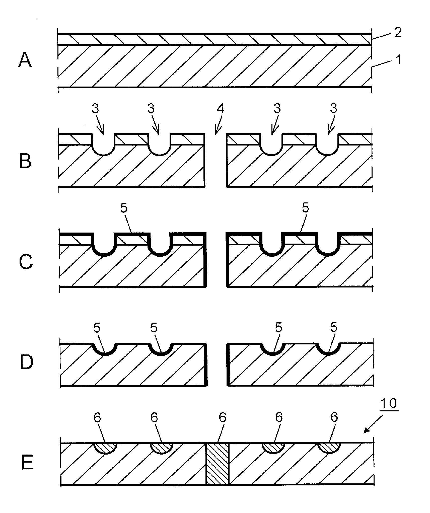
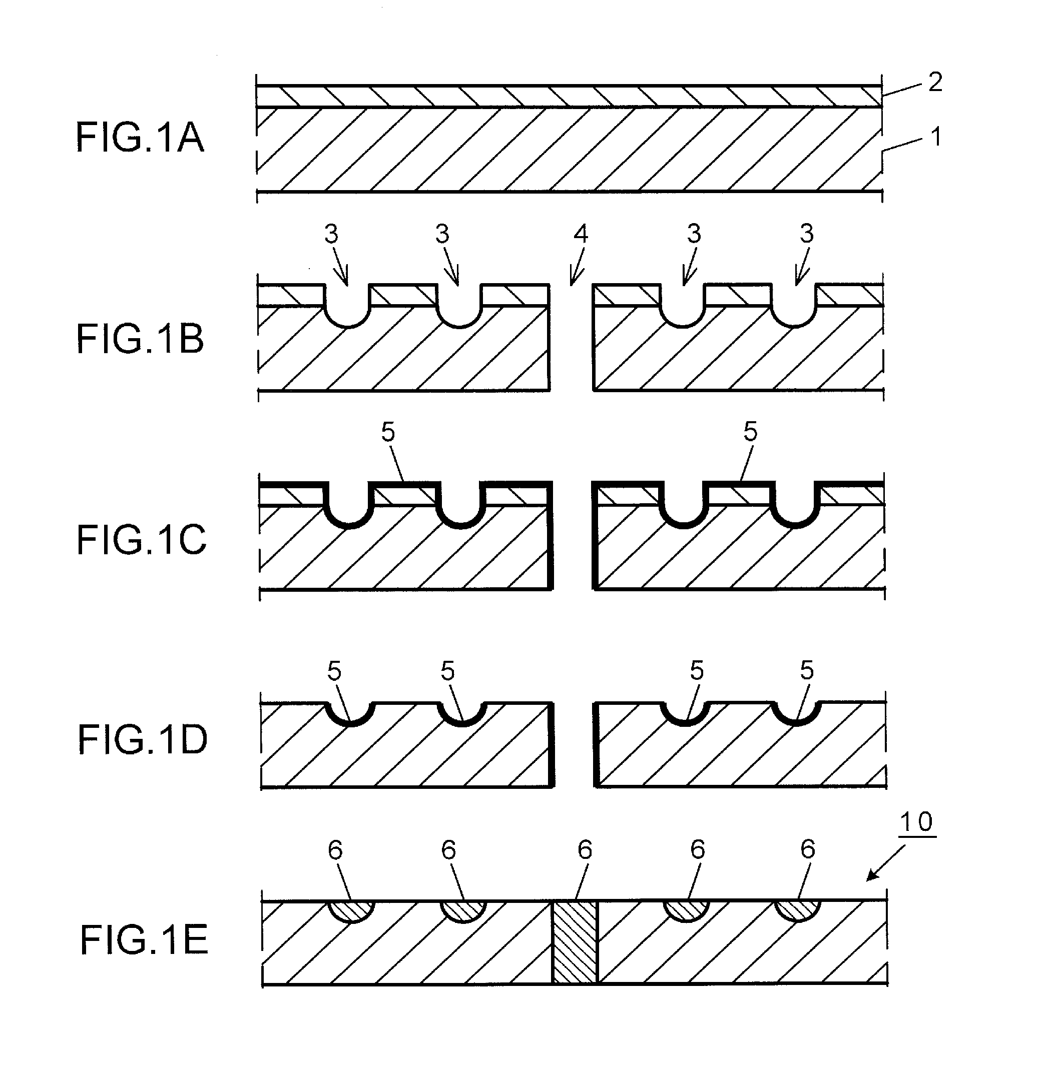
[0147]The invention is described more fully below by way of examples. However, the scope of the invention is not to be understood as being limited in any way by the following examples.

[0148]First, the insulating substrate was fabricated as follows. That is, a release film (TN100, from Toyobo Co., Ltd.) was placed on the surface of a resin substrate made of a resin composition containing a bisphenol A-type epoxy resin (850S, from DIC Corporation), dicyandiamide as a curing agent (DICY, from Nippon Carbide Industries Co., Inc.), 2-ethyl-4-methylimidazozle as a curing accelerator (2E4MZ, from Shikoku Chemical Corporation), silica as an inorganic filler (FB1SDX, from Denki Kagaku Kogyo KK), and methyl ethyl ketone (MEK) and N,N-dimethylformamide (DMF) as solvents. The resulting assembly was molded under applied heat and pressure, then dried under heating, thereby curing the resin substrate. The release film was then peeled off, thereby producing an insulating substrate having a thicknes...


PUM

PropertyMeasurementUnit
Percent by massaaaaaaaaaa
Fractionaaaaaaaaaa

Abstract

The present invention relates to a resin composition which includes a copolymer consisting of a first monomer containing a monomer unit having at least one carboxyl group and a second monomer copolymerizable with the first monomer, and also includes an ultraviolet absorber. The resin composition used is a resin composition for which, when ∈1 represents an absorbance coefficient per unit weight of a resin film 2 in a solution prepared by dissolving, in a solvent, the resin film 2 formed by application of the resin composition as a liquid, ∈1 at a light wavelength at which the resin film 2 is to be irradiated is at least 0.01 (L/(g·cm)).

Description

TECHNICAL FIELD[0001]The present invention relates to a resin composition and a method for producing a circuit board.BACKGROUND ART[0002]In recent years, the increasingly high density of electrical circuits in the field of electricity and electronics has been accompanied by a shift towards finer linewidths and narrower spaces between lines. However, as spaces between lines become narrower, shorts between lines and electromigration tend to arise.[0003]The following circuit board production method is disclosed in Patent Document 1 as art capable of addressing this problem. First, a resin film is formed on the surface of an insulating substrate (resin film forming step). Next, a circuit pattern is created by forming recessed portions having a depth, with reference to an outer of the resin film, which is equal to or greater than the thickness of the resin film (circuit forming step). Then a plating catalyst or a precursor thereof is deposited on the surface of the circuit pattern and th...

Claims


Application Information

Patent Timeline
IPC IPC(8): H05K1/03H05K3/00C08K5/00C08L33/02H05K3/10H05K3/18
CPCH05K1/0353H05K3/0014C08K5/005C08K5/3475C09D125/08C09D133/08C08L33/02H05K3/0032H05K3/107H05K3/184H05K2201/0112H05K2201/0209H05K2201/0239H05K2203/0264H05K2203/0565H05K2203/0571H05K3/0026C08K5/00C08L101/08H05K1/03
Inventor KONNO, YUKOTAKASHITA, HIROMITSUTAKEDA, TSUYOSHIFUJIWARA, HIROAKIYOSHIOKA, SHINGO
Owner PANASONIC CORP
Why Eureka
Try Eureka