Organic light-emitting device and organic light-emitting display apparatus including the same
a technology of light-emitting display apparatus and light-emitting device, which is applied in the direction of electroluminescent light source, thermoelectric device, electric lighting source, etc., can solve problems such as misalignment, and achieve the effect of improving driving voltage characteristics and less misalignmen
- Summary
- Abstract
- Description
- Claims
- Application Information
AI Technical Summary
Benefits of technology
Problems solved by technology
Method used
Image
Examples
example 1
[0155]To manufacture an anode, a corning 15 Ω / cm2 (1200 Å) ITO glass substrate was cut to a size of 50 mm×50 mm×0.7 mm and then sonicated in isopropyl alcohol and pure water each for five minutes, and then cleaned by ultrasonication, followed by ultraviolet (UV) irradiation for about 30 minutes, and exposure to ozone for washing. The resulting glass substrate was loaded into a vacuum deposition device.
[0156]2-TNATA was deposited on the ITO glass substrate to form an HIL having a thickness of about 600 Å on the anode, and then 4,4′-bis[N-(1-naphthyl)-N-phenylamino]biphenyl (NPS) was vacuum-deposited on the HIL to form a HTL having a thickness of about 600 Å.
[0157]DPVBi as a host and Zn(BOX)2 were co-deposited on the HTL in a weight ratio of about 98:2 to form a common blue organic EML having a thickness of about 200 Å.
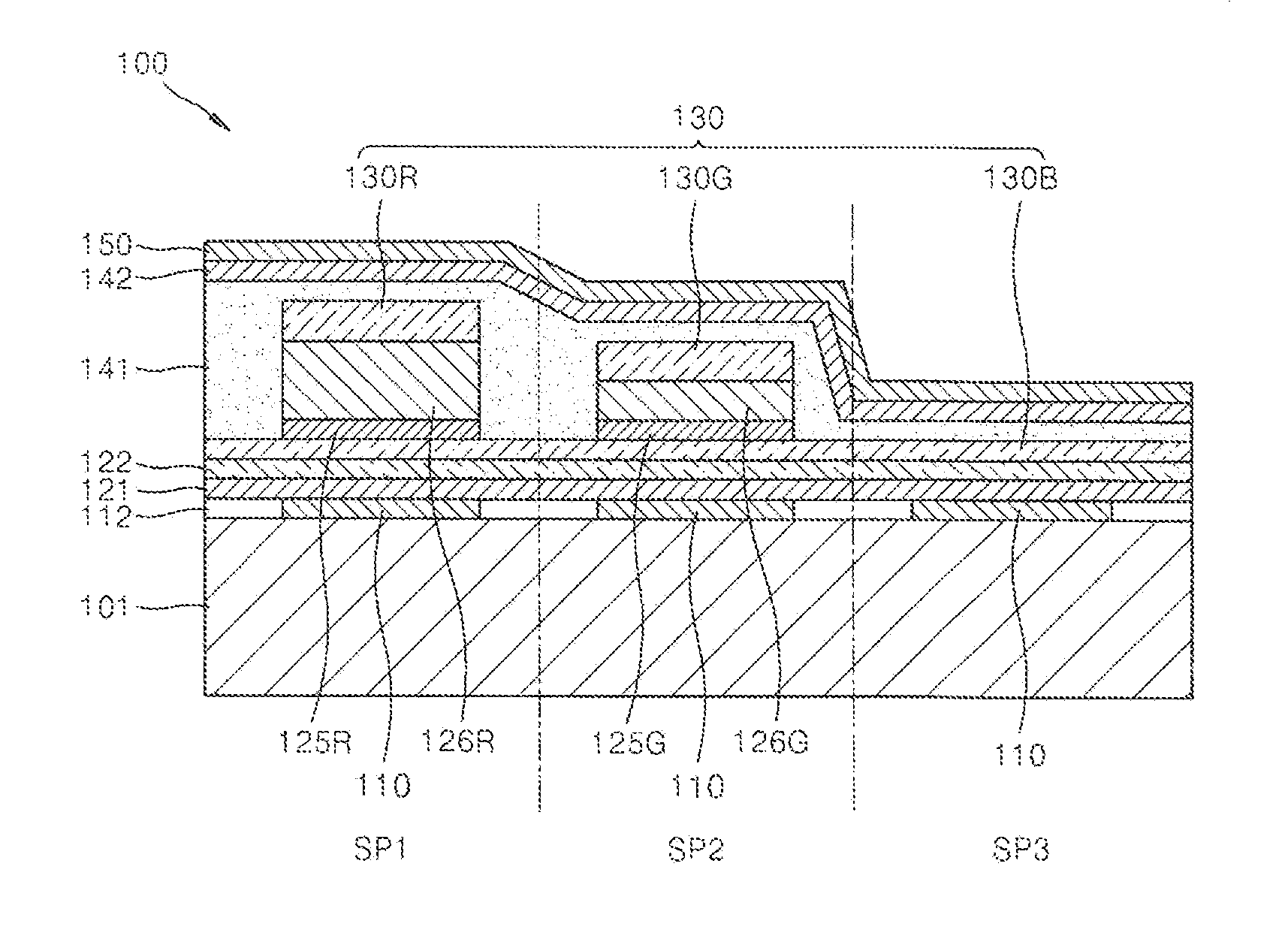
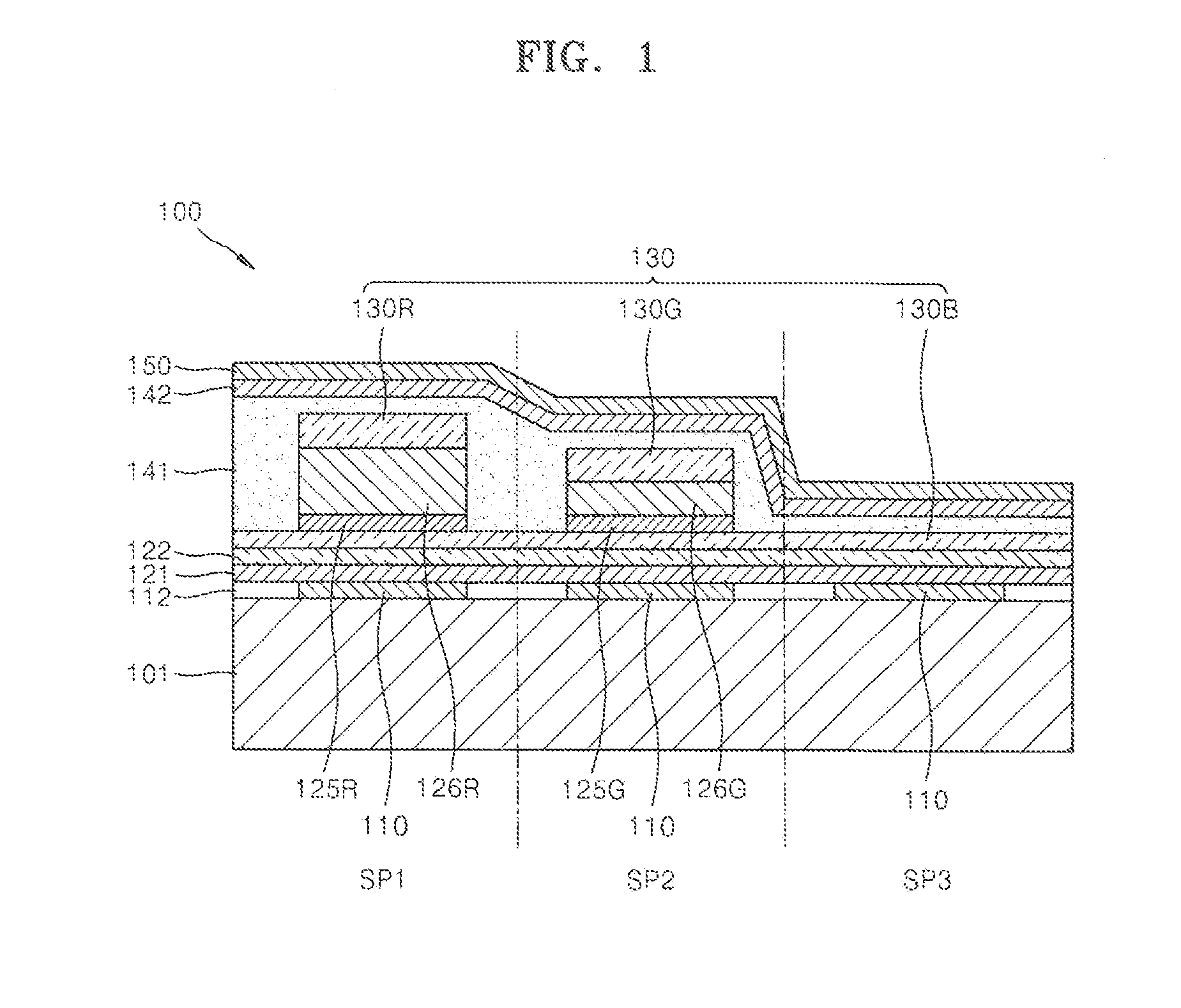
[0158]Subsequently, NPB and Compound 201B were co-deposited on the blue organic EML in a red sub-pixel region in a weight ratio of about 97:3 to form a first doping aux...
example 2
[0162]An organic light-emitting device was manufactured in the same manner as in Example 1, except that a first charge generation layer and a second charge generation layer were further formed as follows.
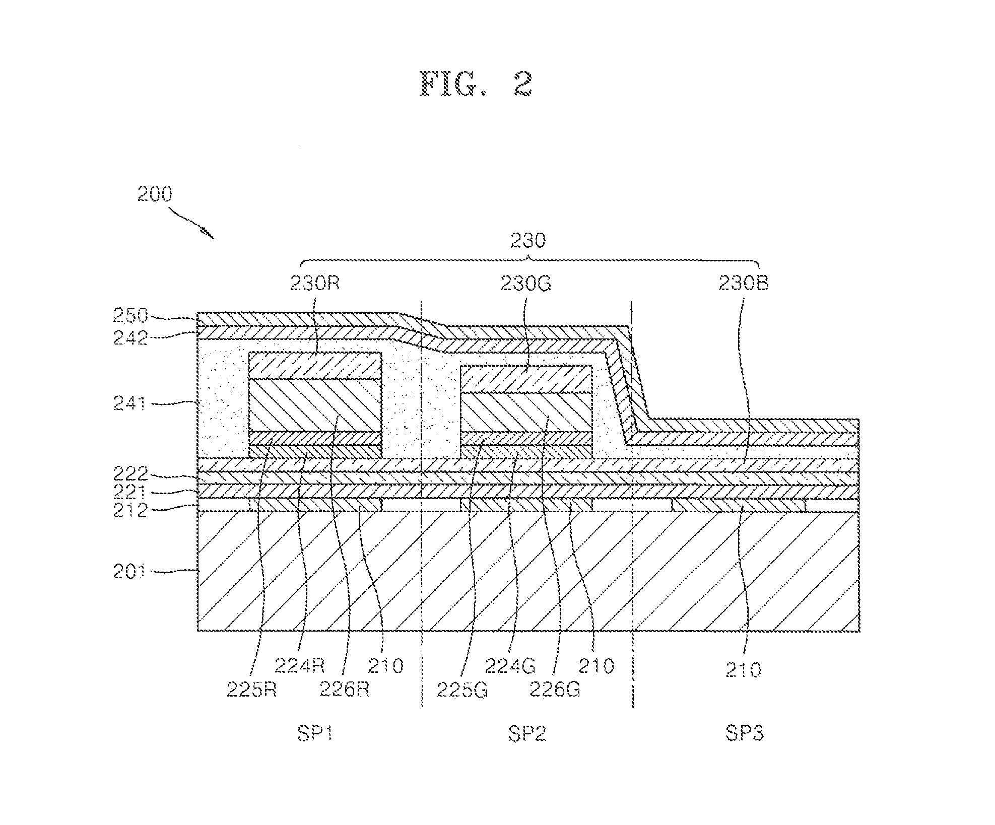
[0163]HAT-CN were deposited on the blue organic EML in a red sub-pixel region to form a first charge generation layer having a thickness of about 50 Å, followed by co-depositing NPB and Compound 201B on the first charge generation layer in a weight ratio of about 97:3 to form a first doping auxiliary layer having a thickness of about 70 Å, depositing NPB on the first doping auxiliary layer to form a first resonance auxiliary layer having a thickness of about 550 Å, and co-depositing Gaq3 as a host and DCJTB as a red dopant on the first resonance auxiliary layer in a weight ratio of about 98:2 thereby forming a red organic EML having a thickness of about 400 Å.
[0164]HAT-CN were deposited on the blue organic EML in a green sub-pixel region to form a second charge generation layer havi...
example 3
[0165]An organic light-emitting device was manufactured in the same manner as in Example 1, except that a first upper resonance auxiliary layer and a first lower resonance auxiliary layer, instead of the first resonance auxiliary layer, and a second upper resonance auxiliary layer and a second lower resonance auxiliary layer, instead of the second resonance auxiliary layer, were formed as follows.
[0166]NPB was deposited on the blue organic EML in a red sub-pixel region to form a first lower resonance auxiliary layer having a thickness of about 50 Å, followed by co-depositing NPB and Compound 201B in a weight ratio of about 97:3 on the first lower resonance auxiliary layer to form a first doping auxiliary layer having a thickness of about 70 Å, depositing NPB on the first doping auxiliary layer to form a first upper resonance auxiliary layer having a thickness of about 550 Å, and co-depositing Gaq3 as a host and DCJTB as a red dopant in a weight ratio of about 98:2 on the first upper...
PUM
 Abstract
Description
Claims
Application Information


