Method for manufacturing silicon carbide substrate

Inactive Publication Date: 2014-01-30
SUMITOMO ELECTRIC IND LTD
View PDF4 Cites 4 Cited by
  • Summary
  • Abstract
  • Description
  • Claims
  • Application Information

AI Technical Summary

Benefits of technology

The present invention provides a method for manufacturing silicon carbide substrates with high quality. The method involves etching the main surface of the seed substrate through two steps: a first step to remove silicon atoms and a second step to remove carbon atoms. This etching process increases the amount of damage to the seed substrate compared to conventional methods, allowing for sufficient removal of the damage layer and reducing the occurrence of crystal defects in the final product. Overall, the method results in a silicon carbide substrate that meets quality standards.

Problems solved by technology

In the sublimation recrystallizing method, when a damage layer such as a polishing flaw exists in a seed substrate's crystal growth surface on which a silicon carbide single crystal is to be grown, the damage layer will cause crystal defects in the silicon carbide single crystal, disadvantageously.
Because each of the methods proposed in Patent Literature 1 to Patent Literature 5 is capable of removing only a small amount of a region including the crystal growth surface of the seed substrate, it is difficult to sufficiently remove the damage layer existing in the crystal growth surface.
Meanwhile, in the method proposed in Patent Literature 6, the crystal growth surface of the seed substrate is not uniformly etched, so that it is difficult to sufficiently remove the damage layer from all over the crystal growth surface.
Thus, the methods proposed in Patent Literature 1 to Patent Literature 6 are not capable of sufficiently removing the damage layer existing in the crystal growth surface of the seed substrate.
Accordingly, it is difficult to manufacture a silicon carbide substrate having high quality.

Method used


Image

  • Method for manufacturing silicon carbide substrate
  • Method for manufacturing silicon carbide substrate
  • Method for manufacturing silicon carbide substrate

Examples


example

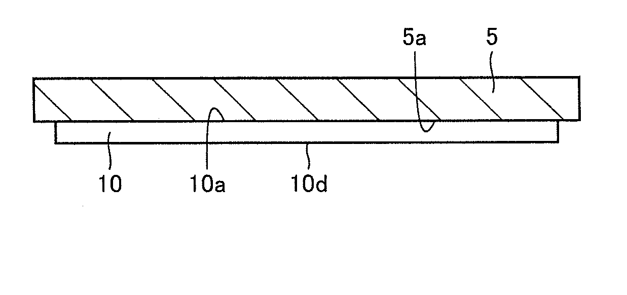
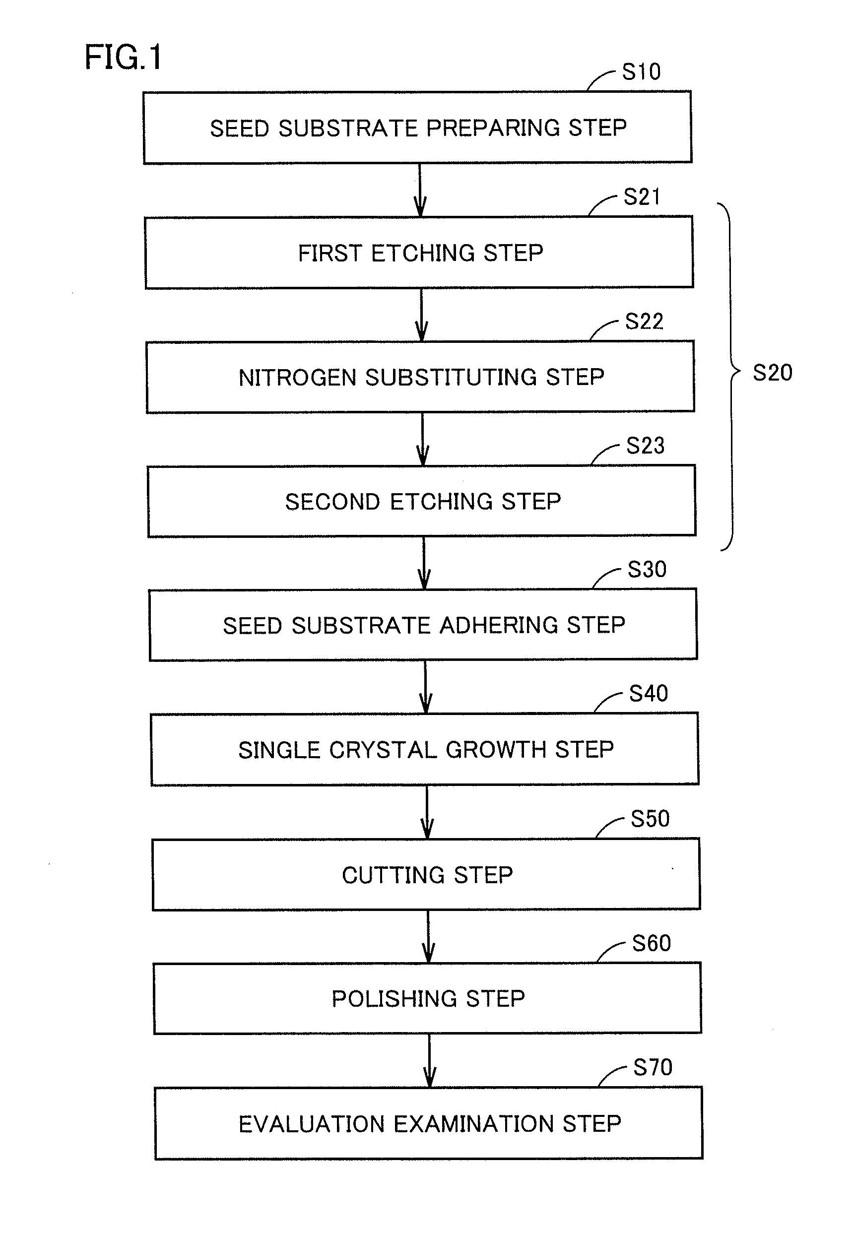
[0049]An experiment was conducted to confirm the effect of the present invention with regard to quality of the silicon carbide substrate. First, a seed substrate having a diameter of 2 inches and made of silicon carbide was prepared. Next, the seed substrate thus prepared was placed in an etching chamber of a reaction tube such that its main surface to be etched faced upward. The etching chamber had a volume of 14 L. Next, the etching chamber was vacuumed to reduce pressure to 50 Pa. Next, while maintaining the vacuum state in the etching chamber, temperature therein was increased to 1000° C. Next, chlorine gas was introduced into the etching chamber. The chlorine gas was introduced at a flow rate of 0.3 L / min for 30 minutes. Next, the etching chamber was vacuumed and the gas in the etching chamber was substituted with nitrogen gas. Next, oxygen gas was introduced into the etching chamber. The oxygen gas was introduced at a flow rate of 2 L / min for 5 minutes. Then, a change in the t...


PUM


Abstract

A method for manufacturing a silicon carbide substrate includes the steps of: preparing a seed substrate made of silicon carbide; etching a main surface of the seed substrate prepared; obtaining an ingot by growing a silicon carbide single crystal film on a crystal growth surface formed by etching the main surface of the seed substrate;and obtaining a silicon carbide substrate by cutting the ingot. The step of etching the seed substrate includes: a first etching step of removing silicon atoms, which form the silicon carbide, from an etching region using chlorine gas, the etching region being a region including the main surface of the seed substrate; and a second etching step of removing carbon atoms, which form the silicon carbide, from the etching region from which the silicon atoms have been removed, using oxygen gas.

Description

BACKGROUND OF THE INVENTION[0001]1. Field of the Invention[0002]The present invention relates to a method for manufacturing a silicon carbide substrate, more particularly, a method for manufacturing a silicon carbide substrate having high quality.[0003]2. Description of the Background Art[0004]In recent years, in order to achieve high breakdown voltage, low loss, and the like in a semiconductor device, silicon carbide has begun to be adopted as a material for the semiconductor device. Silicon carbide is a wide band gap semiconductor having a band gap larger than that of silicon, which has been conventionally widely used as a material for semiconductor devices. Hence, by adopting silicon carbide as a material for a semiconductor device, the semiconductor device can have a high breakdown voltage, reduced on-resistance, and the like.[0005]In such a semiconductor device employing silicon carbide as its material, a substrate made of silicon carbide is used. The silicon carbide substrate ...

Claims


Application Information

Patent Timeline
IPC IPC(8): H01L21/02
CPCH01L21/02529C30B23/00C30B29/36
Inventor HONKE, TSUBASANISHIGUCHI, TAROHORI, TSUTOMU
Owner SUMITOMO ELECTRIC IND LTD
Why Eureka
Try Eureka