Split embedded dram processor

a processor and embedded technology, applied in the field of microprocessors and embedded dram architectures, can solve the problems of large amount of data traffic between the memory and the processor, inability to build caches large enough to hold, and inability to so as to minimize data bussing traffic and achieve the effect of effectively cache instructions and data

Inactive Publication Date: 2014-01-30
DOWLING ERIC M
View PDF4 Cites 2 Cited by
  • Summary
  • Abstract
  • Description
  • Claims
  • Application Information

AI Technical Summary

Benefits of technology

This patent describes a processing architecture that combines a CPU core and an embedded DRAM chip to efficiently handle memory-intensive tasks. The architecture is designed to be transparent to the programmer, allowing standard software to run on the processor. It takes advantage of the embedded DRAM, which has multiple address spaces that minimize data bussing traffic between the processors. The architecture allows for easy upgrading in the field by inserting an embedded DRAM module into an existing slot and adding accelerators to standard software. In one embodiment, a profiler analyzes uniprocessor execution and constructs modification tables to reassign certain code segments to the embedded DRAM coprocessor. The embedded DRAM also monitors the instruction stream and performs memory-intensive tasks, reducing the amount of traffic that needs to be bussed back and forth between the CPU core and the embedded DRAM chips. The architecture also includes a specialized video and graphics processing system. Standard software can be accelerated either with or without the express knowledge of the processor. Overall, this technology improves processing efficiency by optimizing memory usage and reducing data bussing traffic.

Problems solved by technology

The fact that DRAM access times do not double every few years results in a processor-DRAM speed mismatch.
Especially with video and image data, it is not practical to build caches large enough to hold the requisite data structures while they are being processed.
This gives rise to large amounts of data traffic between the memory and the processor and decreases cache efficiency.
However, even with faster synchronous DRAM, the problem remains that performance is limited by the DRAM access time needed to transfer data to and from the processor.
In these situations, cache performance diminishes as the processor is burdened with having to manipulate large data structures distributed across large areas in memory.
In many cases, these memory accesses are interleaved with disk accesses, further reducing system performance.
However, the coprocessor is external from the memory, and no increase in effective memory bandwidth is realized.
Also, this solution does not provide for the important situation when the CPU involves a cache.
Another deficiency with this prior art is its inability to provide a solution for situations where the processor is not aware of the presence of the coprocessor.
Furthermore, it does not define a protocol to allow the coprocessor to interact with the instruction sequence before it arrives at the processor.
This interface concept is not sufficient to support the features and required performance needed of the embedded DRAM coprocessors.
Moreover, introduction of a large task switching overhead eliminates the acceleration advantages.
While this system may be used as an attached vector processor, it does not serve to accelerate the normal software executed on a host processor.
This architecture does not provide a tightly coupled acceleration unit that can accelerate performance with specialized instruction set extensions, and it cannot be used to accelerate existing applications software unaware of the existence of the embedded DRAM coprocessor.

Method used


Image

  • Split embedded dram processor
  • Split embedded dram processor
  • Split embedded dram processor

Examples


Embodiment Construction

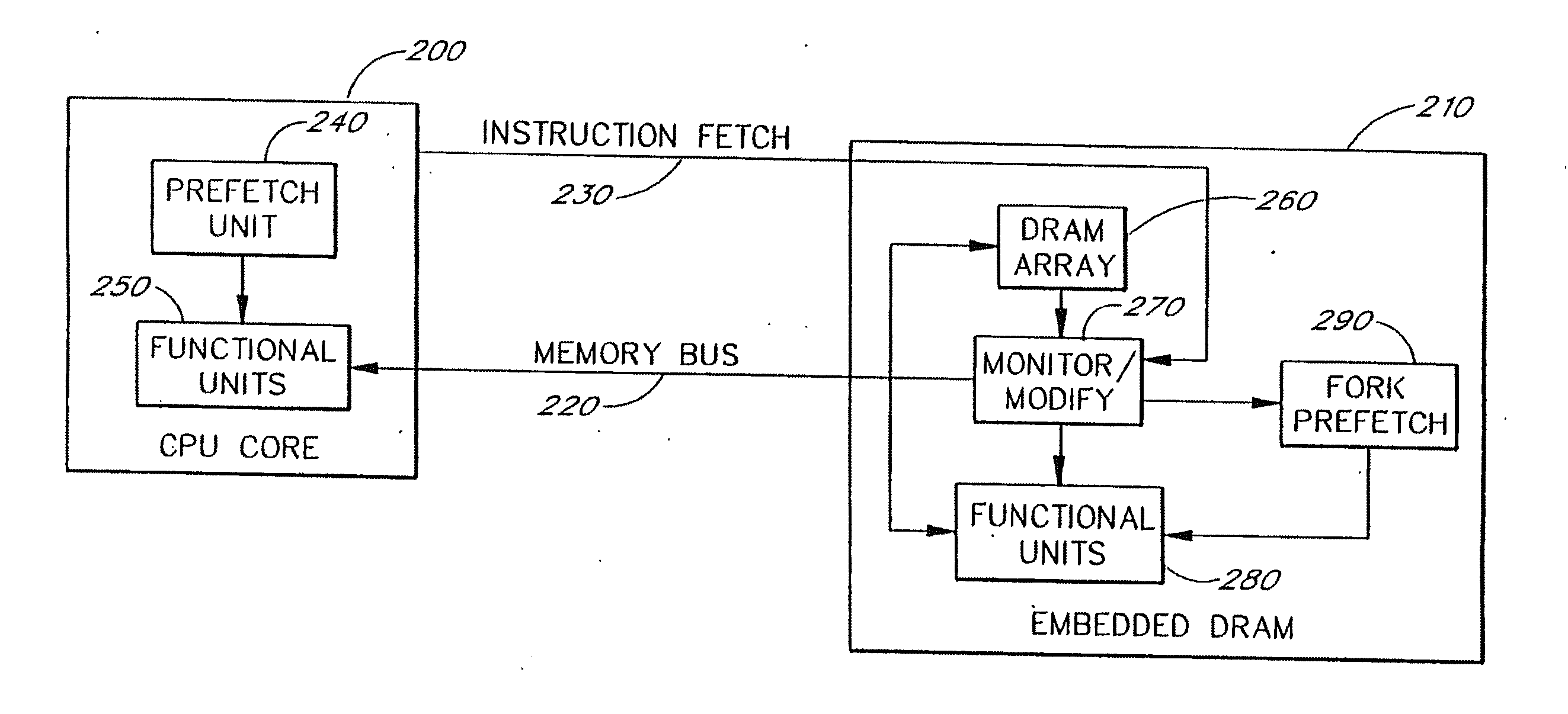
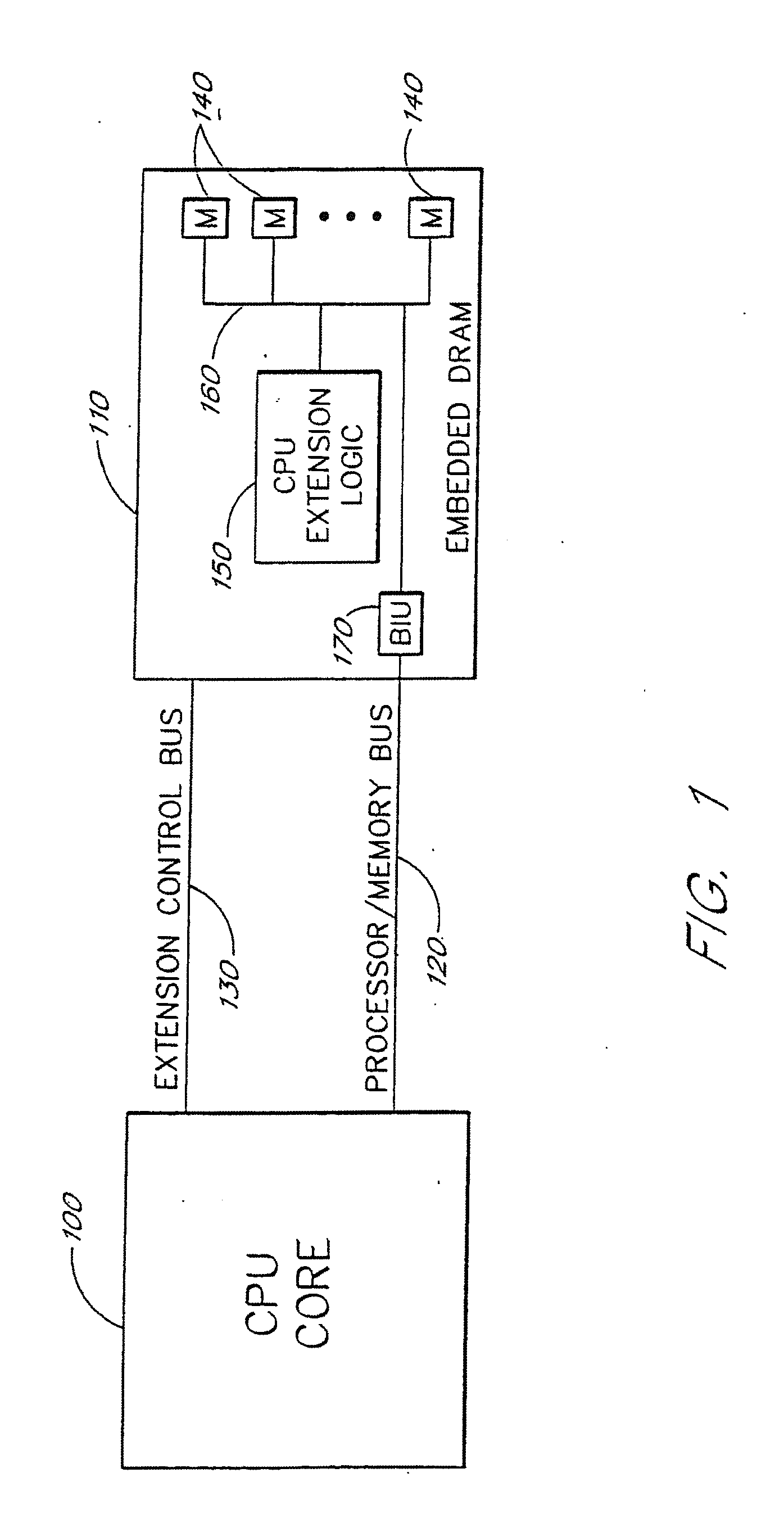
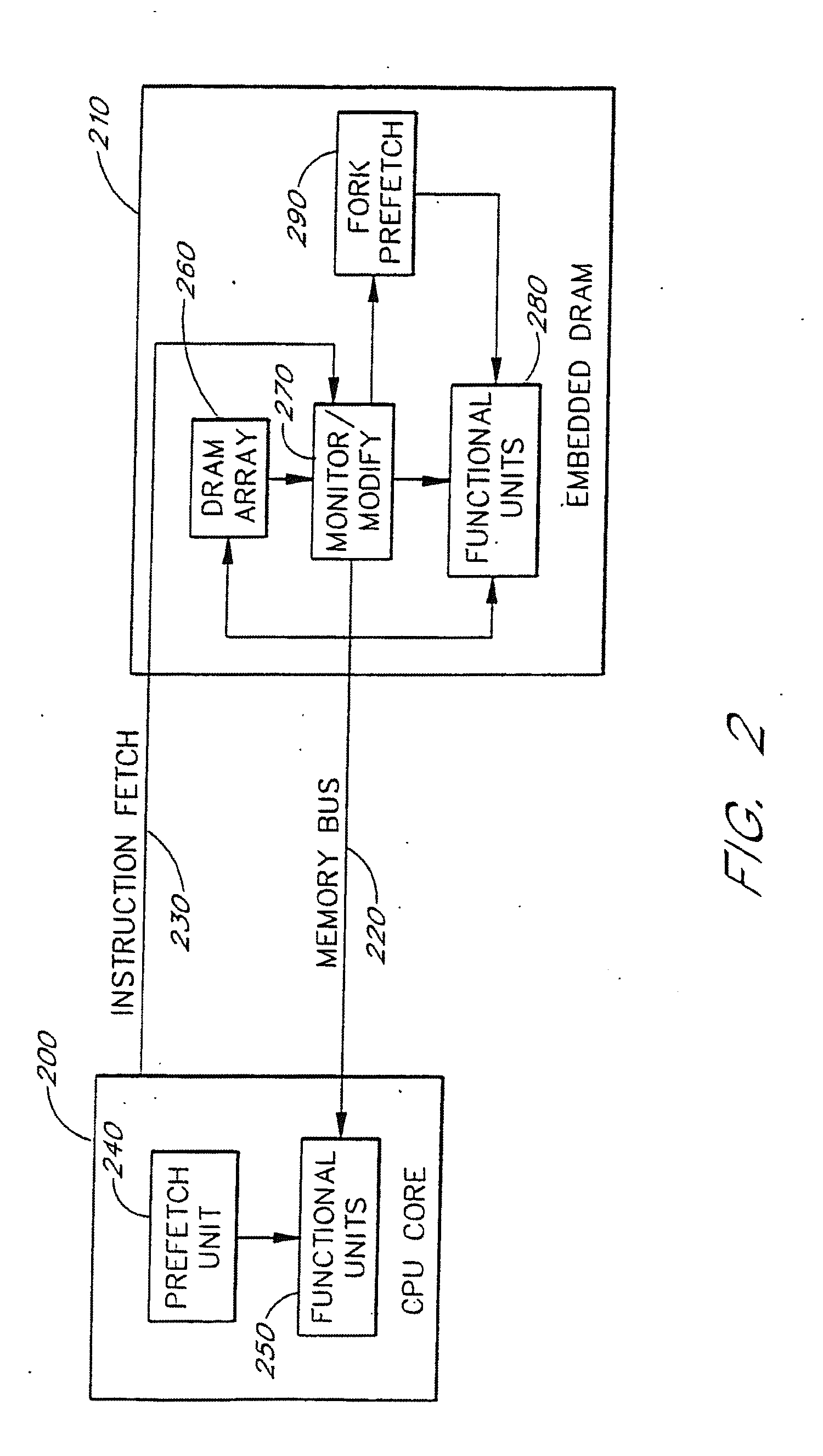
[0056]FIG. 1 is a high level block diagram of an embodiment of a split architecture comprising a CPU 100 with an embedded DRAM extension 110 according to the present invention. The CPU 100 is coupled to the embedded DRAM 110 via a standard memory bus connection 120 and an optional extension control bus 130. The embedded DRAM 110 includes a DRAM memory array 140 which is coupled to an embedded logic CPU extension 150 via an internal bussing structure 160. Data transfers between internal bus 160 and external bus 120 are bidirectionally buffered and optionally queued by bus interface unit (BIU) 170. External transactions over the bus 120 are controlled via external control signals generated by the CPU 100 or via internal control signals generated by the CPU extension 150. In this system, the memory interface bus 120 carries address and control information to and possibly from the memory, and carries data back and forth between the CPU 100 and the embedded DRAM 110. The memory interface...


PUM


Abstract

A processing architecture includes a first CPU core portion coupled to a second embedded dynamic random access memory (DRAM) portion. These architectural components jointly implement a single processor and instruction set. Advantageously, the embedded logic on the DRAM chip implements the memory intensive processing tasks, thus reducing the amount of traffic that needs to be bussed back and forth between the CPU core and the embedded DRAM chips. The embedded DRAM logic monitors and manipulates the instruction stream into the CPU core. The architecture of the instruction set, data paths, addressing, control, caching, and interfaces are developed to allow the system to operate using a standard programming model. Specialized video and graphics processing systems are developed. Also, an extended very long instruction word (VLIW) architecture implemented as a primary VLIW processor coupled to an embedded DRAM VLIW extension processor efficiently deals with memory intensive tasks. In different embodiments, standard software can be accelerated either with or without the express knowledge of the processor.

Description

CROSS-REFERENCE TO RELATED APPLICATIONS[0001]The present application is a divisional of U.S. patent application Ser. No. 10 / 884,132 filed Jul. 2, 2004, entitled “Split Embedded DRAM Processor,” which is a continuation of U.S. patent application Ser. No. 09 / 652,638 filed Aug. 31, 2000, now U.S. Pat. No. 6,760,833, which issued on Jul. 6, 2004, which is a continuation of U.S. patent application Ser. No. 09 / 487,639 filed Jan. 19, 2000, now U.S. Pat. No. 6,226,736, which issued on May 1, 2001, which is a divisional of U.S. patent application Ser. No. 08 / 997,364 filed Dec. 23, 1997, now U.S. Pat. No. 6,026,478, which issued on Feb. 15, 2000.BACKGROUND OF THE INVENTION[0002]1. Field of the Invention[0003]The present invention relates to the fields of microprocessor and embedded DRAM architectures. More particularly, the invention pertains to a split processor architecture whereby a CPU portion performs standard processing and control functions, an embedded DRAM portion perform memory-inte...

Claims


Application Information

Patent Timeline
Patent Type & Authority Applications(United States)
IPC IPC(8): G06F15/78G06F9/38
CPCG06F15/7839G06F9/3842G06F9/3853G06F9/3877G06F9/3885
Inventor DOWLING, ERIC M.
Owner DOWLING ERIC M
Why Eureka
Try Eureka