Piezoelectric element, piezoelectric device and method of manufacturing piezoelectric element

Inactive Publication Date: 2014-02-13
SORIN CRM +1
View PDF4 Cites 24 Cited by
  • Summary
  • Abstract
  • Description
  • Claims
  • Application Information

AI Technical Summary

Benefits of technology

[0042]According to one embodiment of the invention, a piezoelectric element can be stably provided that has a piezoelectric film comprised of lead-free materials such as lithium potassium sodium niobate and that has an excellent piezoelectric property by controlling the local structure (binding state of the atoms) of the piezoelectric film with a high degree of accuracy, as well as a piezoelectric device using the piezoelectric element.
[0043]In addition, the piezoelectric element according to the embodiment of the invention makes it possible to prevent the yield from being lowered, when a Pt electrode or a Pt alloy electrode of which crystal orientation is controlled is used as the lower electrode

Problems solved by technology

This technique is, in principle, configured to form the piezoelectric film under high vacuum, thus oxygen in the oxide thin film is likely to be scarce, consequently it is subjected to the disadvantages of stoichiometrically causing a composition misalignment or the like in comparison with a raw material target.
Furthermore, in the conventional technique, in a lead-free based piezoelectric film corresponding to a basic portion of the piezoelectric eleme

Method used


Image

  • Piezoelectric element, piezoelectric device and method of manufacturing piezoelectric element
  • Piezoelectric element, piezoelectric device and method of manufacturing piezoelectric element
  • Piezoelectric element, piezoelectric device and method of manufacturing piezoelectric element

Examples


examples

[0107]Examples according to the invention will be explained below.

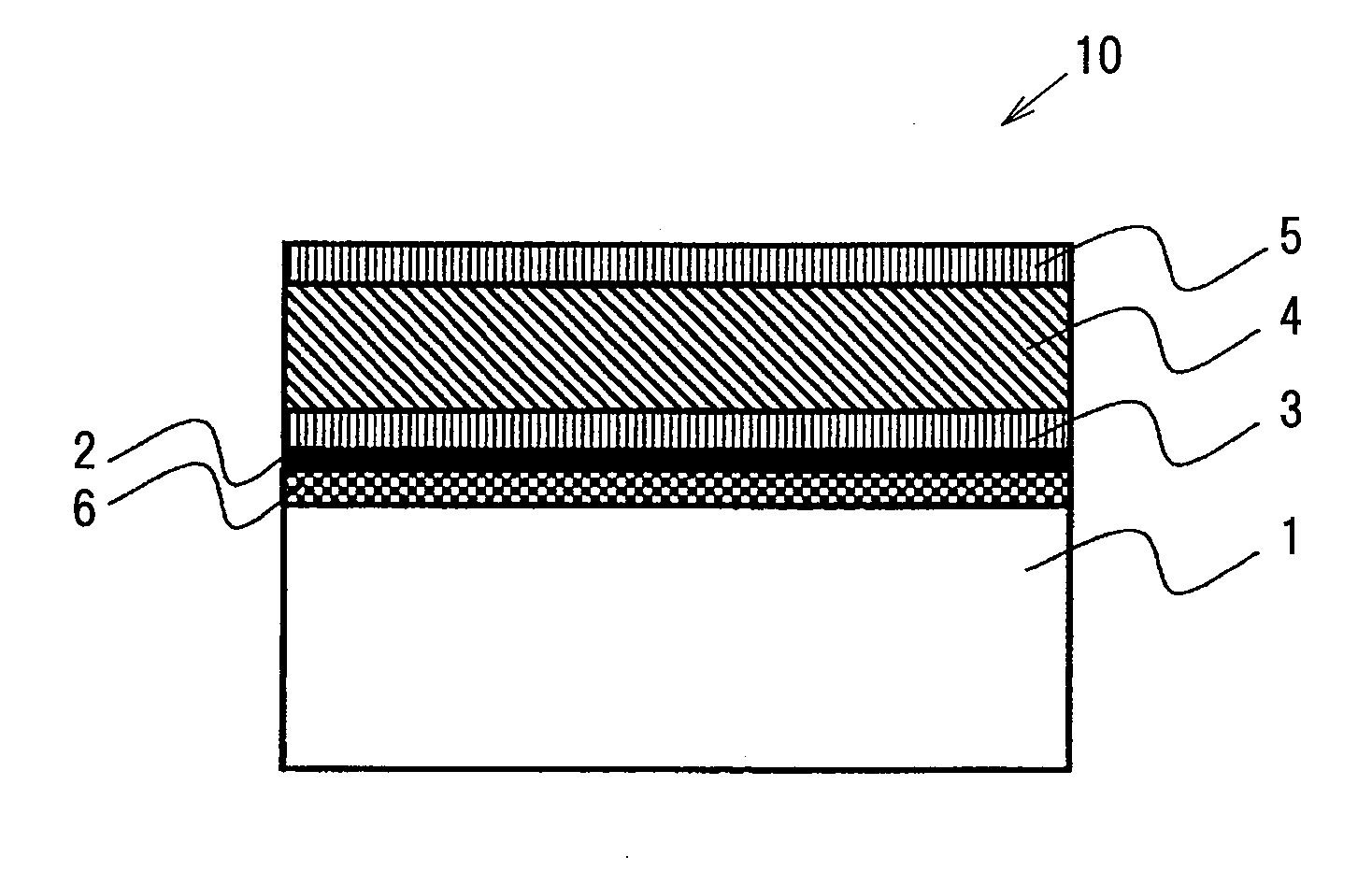
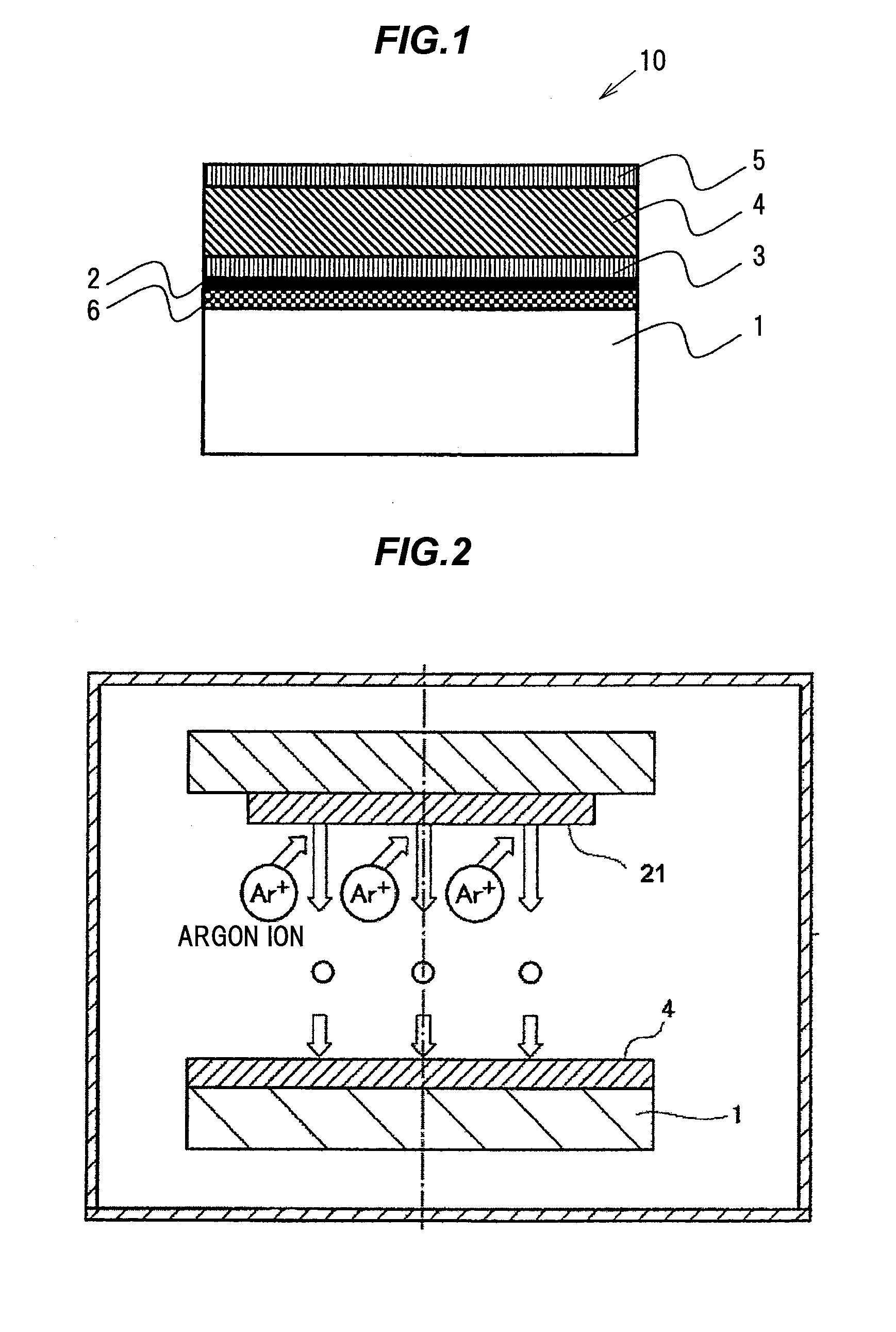
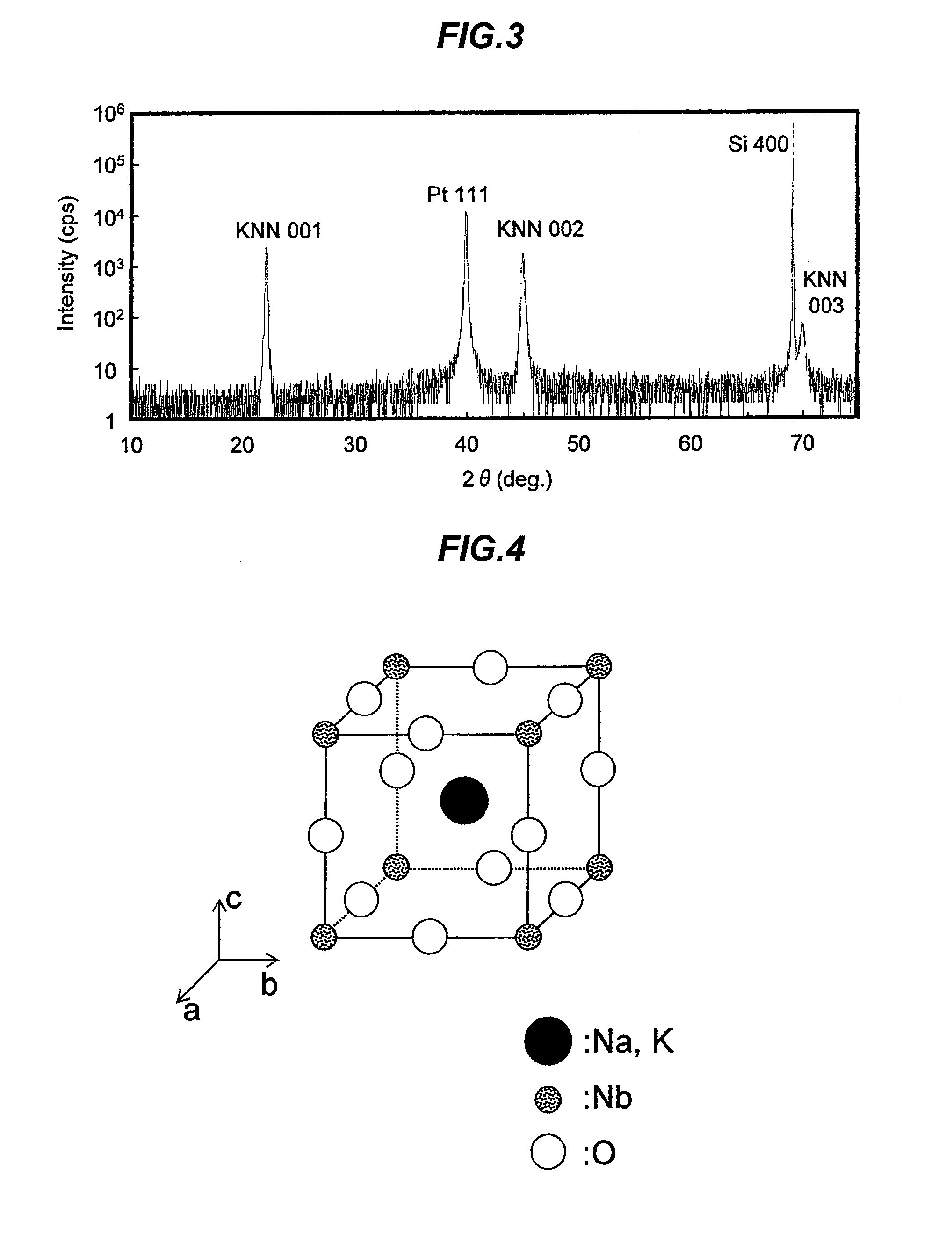
[0108]FIG. 1 is a cross-sectional view schematically showing a substrate with a piezoelectric element. In the Example, the piezoelectric element 10 was manufactured such that the adhesion layer 2 was formed directly on the substrate or on the substrate via the oxidized film 6, and the lower electrode layer 3, the piezoelectric film 4 comprised of a perovskite type potassium sodium niobate (hereinafter referred to as “KNN”) and the upper electrode layer 5 were formed on the adhesion layer 2. The content of an organic molecule and a molecule having a hydroxyl group in the piezoelectric film 4 is changed dependent on the crystal condition, the composition and the manufacturing condition of the piezoelectric film 4. Hereinafter, a manufacturing method will be explained in detail.

[0109]First, a thermally-oxidized film (the oxidized film 6) was formed on the Si substrate 1, and the adhesion layer 2 comprised of a Ti film of...


PUM

PropertyMeasurementUnit
Energyaaaaaaaaaa
Thicknessaaaaaaaaaa
Electric potential / voltageaaaaaaaaaa

Abstract

A piezoelectric element includes a substrate, and a lower electrode layer, a piezoelectric film represented by a general formula of (NaxKyLiz)NbO3 (0<x≦1, 0<y≦1, 0≦x≦0.2, x+y+z=1) and an upper electrode layer formed on the substrate. The piezoelectric film has a crystal structure of pseudo-cubic crystal, tetragonal crystal, orthorhombic crystal, monoclinic crystal or rhombohedral crystal, or has a state that at least two of the crystal structures coexist. A difference between the maximum value and the minimum value of an energy of Na-K absorption edge measured by an electron energy loss spectroscopy or an X-ray-absorption fine-structure spectroscopy in a direction of the film thickness of the piezoelectric film is not more than 0.8 eV.

Description

[0001]The present application is based on Japanese patent application No. 2012-174837 filed on Aug. 7, 2012, the entire contents of which are incorporated herein by reference.BACKGROUND OF THE INVENTION[0002]1. Field of the Invention[0003]This invention relates to a piezoelectric element configured such that a piezoelectric property is improved by accurately controlling the atomic-level structure of a lead-free piezoelectric film using lithium potassium sodium niobate, a piezoelectric device and a method of manufacturing a piezoelectric element. 2. Description of the Related Art[0004]A piezoelectric element is processed so as to form various piezoelectric devices in accordance with a variety of the intended uses, in particular, is widely used as a functional electronic component such as an actuator that allows an object to be changed in shape when an electric voltage is applied thereto, a sensor that generates an electric voltage due to the change in shape of the element reversely.[...

Claims


Application Information

Patent Timeline
IPC IPC(8): H01L41/18H01L41/22
CPCH01L41/22H01L41/18C01G33/006C30B29/30H01G5/18C01P2002/30C01P2002/34C01P2002/72C01P2004/04C01P2006/40C30B23/025C30B29/22Y10T29/42H10N30/1051H10N30/2042H10N30/8542H10N30/04H10N30/076H10N30/85H10N30/01
Inventor SUENAGA, KAZUFUMISHIBATA, KENJIWATANABE, KAZUTOSHINOMOTO, AKIRAHORIKIRI, FUMIMASA
Owner SORIN CRM
Why Eureka
Try Eureka