
Semiconductor circuit and methodology for in-system scan testing

Active Publication Date: 2014-02-13
ANALOG DEVICES INT UNLTD
View PDF12 Cites 27 Cited by
  • Summary
  • Abstract
  • Description
  • Claims
  • Application Information

AI Technical Summary

Benefits of technology

The present invention provides a scan test method for a semiconductor circuit that allows for the selective writing and reading of bit values and logic states from the register addresses and memory addresses mapped to the bi-directional communication port. This mapping of the address space allows for the selective writing and reading of bit values or logic states from the scan control registers. The scan test program or application can be provided to customers to allow for simple and useful pass / fail mode evaluation of the combinatorial logic block of the semiconductor circuit. The method also allows for the identification of error-prone portions of logic in the semiconductor circuit and the use of a predefined digital test pattern to detect failing devices.

Problems solved by technology

Furthermore, since numerous separate scan-chains coupled to different logic blocks of the digital logic are utilized for typical digital semiconductor circuits, the number of external pins that must be allocated for ATPG testing becomes large.
This feature limits the application of ATPG test methodologies to production test at the wafer level before the semiconductor device is packaged and shipped to the customer.
Hence if the semiconductor device fails, or is suspected to be failing, during board level testing the semiconductor device must be removed from the customer's board when failure analysis is required.
This is a time-consuming and error-prone operation due to the number of pins, small pin pitch and miniscule dimensions of contemporary semiconductor circuits.
The failed semiconductor circuit may consequently be damaged by the PCB removal operation itself.
This can often make it impossible to properly diagnose or analyze the suspected or failed semiconductor device.
Unfortunately, the detection of failures during the initial board level testing is important in virtually all types of applications despite the prior ATPG based production level testing being applied to semiconductor device as explained above.

Method used


Image

  • Semiconductor circuit and methodology for in-system scan testing
  • Semiconductor circuit and methodology for in-system scan testing
  • Semiconductor circuit and methodology for in-system scan testing

Examples


Embodiment Construction

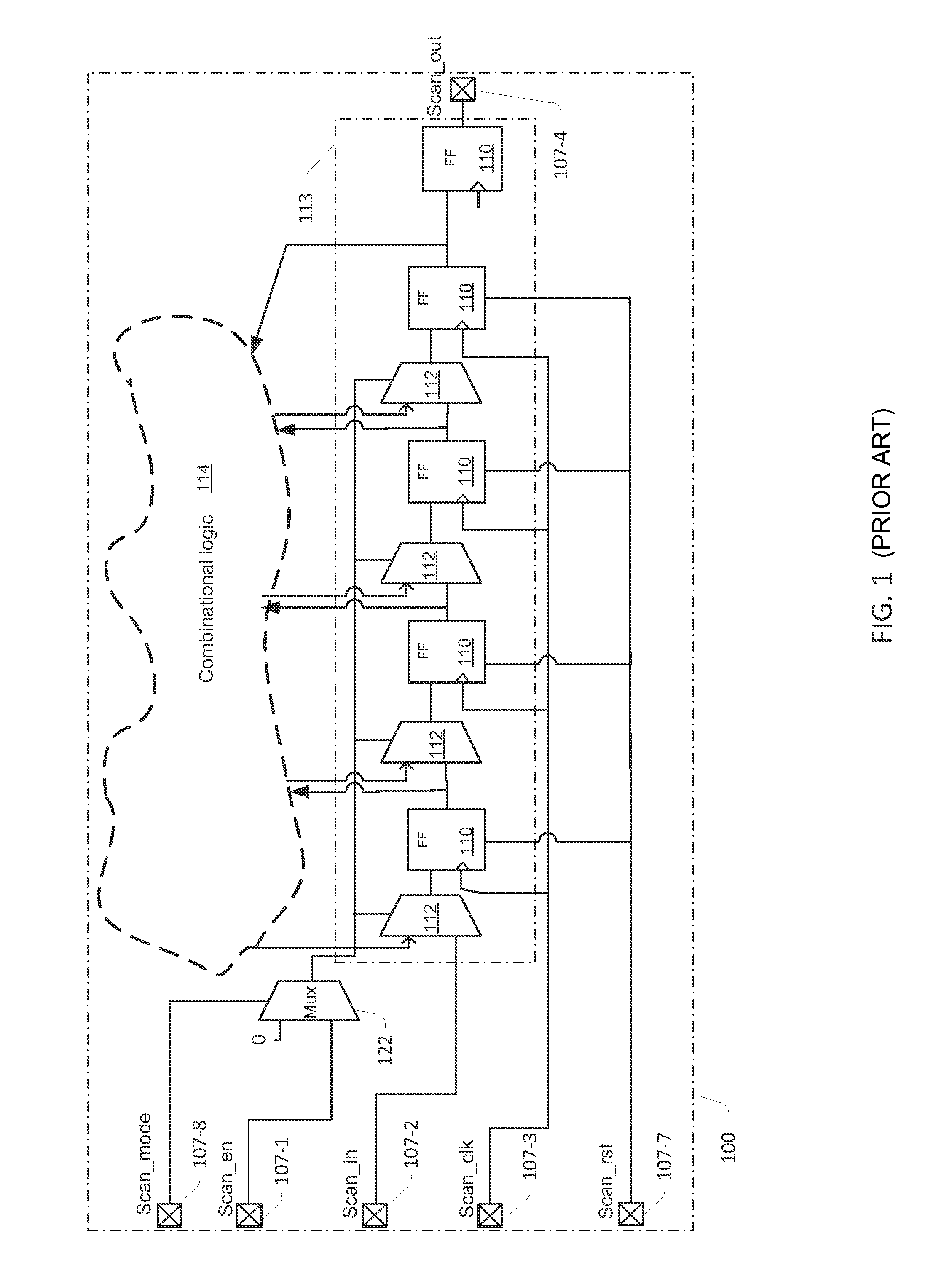
[0036]FIG. 1 is a schematic diagram of a prior art semiconductor device 100 with associated scan test logic and externally accessible scan input and output pads or pins 107-1, 107-2, 107-3, 107-4, 107-7, 107-8. The semiconductor device 100 comprises a digital circuit portion which comprises a combinatorial logic block 114. The combinatorial logic block 114 is coupled to a scan chain 113 which schematically comprises 4 cascaded stages of flip-flops 210 and 4 cascaded multiplexers 212 inserted between outputs and data inputs of the cascaded flip-flops 110. In practice, the scan chain 113 may comprise a much higher or larger number of cascaded stages of flip-flops 110 and multiplexers 112. The scan chain 113 functions like a shift register when the scan mode of the semiconductor circuit 100 is enabled through the external pad 107-8 Scan_mode which is coupled to select inputs of each of the 4 cascaded multiplexers 112 through a scan enable multiplexer 122. In the scan enabled mode, a pr...


PUM


Abstract

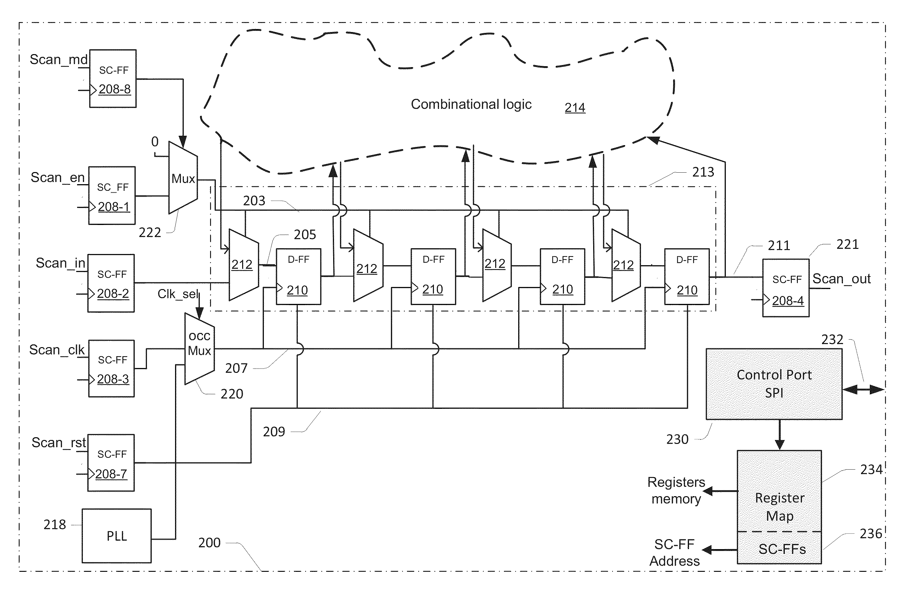
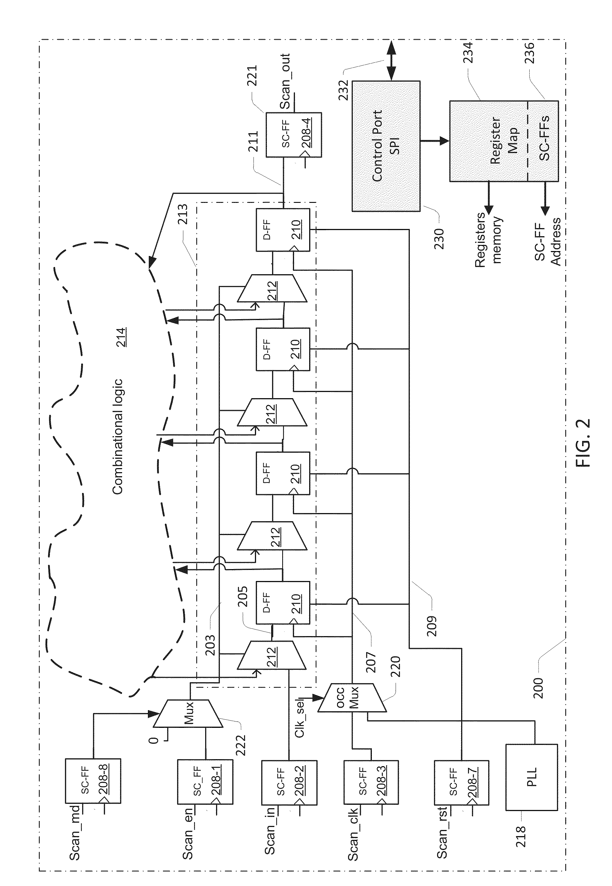
A semiconductor circuit comprising a digital circuit portion, which comprises a combinatorial logic block. The semiconductor circuit further comprises a scan chain for loading and applying a predefined digital test pattern to inputs of the combinatorial logic block. A bi-directional communication port is adapted for writing incoming data to an address space of the digital circuit portion. Scan control hardware comprises a plurality of individually addressable scan control registers which are mapped to the address space of the bi-directional communication port. A method of testing the digital circuit portion involves, using the scan chain, writing bit values to inputs of the individually addressable scan control registers, and reading bit values from at least one output of an individually addressable scan control register. The method and semiconductor circuit allow thorough testing and diagnosing of failing semiconductor devices, including core logic thereof, while mounted on a printed circuit board.

Description

BACKGROUND OF THE INVENTION[0001]The invention provides valuable improvements over existing ATPG (Automated Test Pattern Generation) test methodologies, on-chip scan control hardware and ATE equipment in connection with testing of digital semiconductor devices or integrated circuits (ICs). Existing ATPG test methodologies are widely used in the semiconductor industry for digital IC testing during manufacturing such that defective semiconductor devices can be identified and discarded during production test. The existing ATPG test methodologies can also be used for diagnostic purposes to identify a particular portion of digital logic / gates that often fails such that the error-prone digital logic portion may be redesigned if the yield figures are unacceptable. Existing ATPG test methodologies require the use of numerous externally accessible pins or pads of the semiconductor device to be tested. These external pins are used during production test of the semiconductor device to apply di...

Claims


Application Information

Patent Timeline
IPC IPC(8): G01R31/3177
CPCG01R31/27G01R31/318555
Inventor LAMB, DAVIDFRANZEN, KENDRICK OWEN DANIELHOSSACK, DAVID
Owner ANALOG DEVICES INT UNLTD
Learn More