Semiconductor assembly with dual connecting channels between interposer and coreless substrate

Inactive Publication Date: 2014-02-20
BRIDGE SEMICON
View PDF6 Cites 64 Cited by
  • Summary
  • Abstract
  • Description
  • Claims
  • Application Information

AI Technical Summary

Benefits of technology

[0027]The present invention has numerous advantages. The conductive through via in the interposer can improve power stability of the attached chip. The bond wire can provide alternative interconnection pathway between the interposer and the coreless substrate in addition to the through via residing in the interposer, thereby reducing the number of through-via needed for the interposer. As such, the size of the interposer may be reduced, or the fabrication yield of the through-via can be improved due to lower density of the through-via in the interposer. Therefore, adding bond wire can significantly reduce the cost of the interposer and hence the semiconductor assembly. The stopper of the co

Problems solved by technology

However, in most cases, more than one chip may b

Method used


Image

  • Semiconductor assembly with dual connecting channels between interposer and coreless substrate
  • Semiconductor assembly with dual connecting channels between interposer and coreless substrate
  • Semiconductor assembly with dual connecting channels between interposer and coreless substrate

Examples


embodiment 1

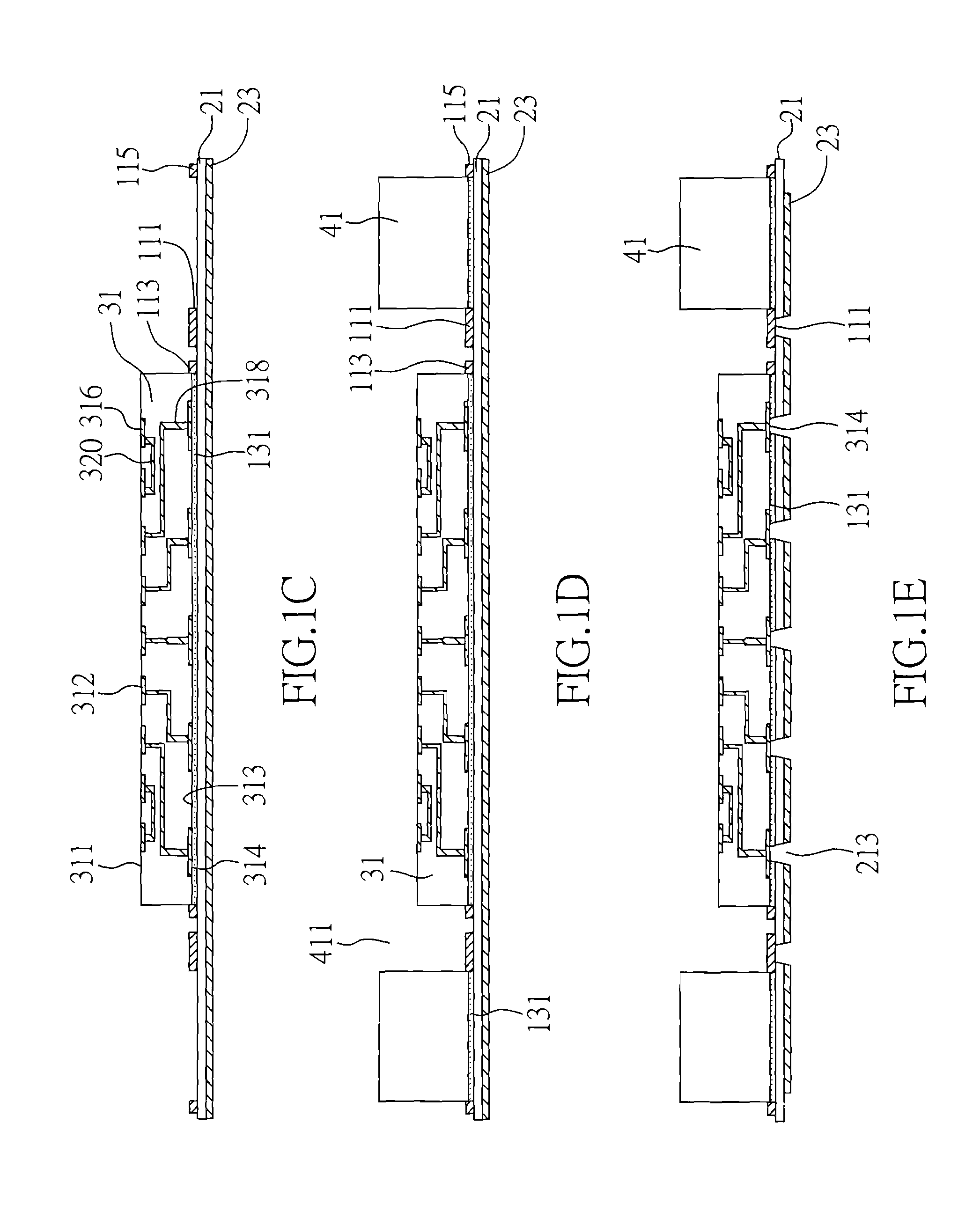
[0034]FIGS. 1A-1J are cross-sectional views showing a method of making a semiconductor assembly that includes an interposer, a semiconductor chip, a stiffener and coreless substrate electrically connected to the interposer by bond wires and conductive micro-vias in accordance with an embodiment of the present invention.

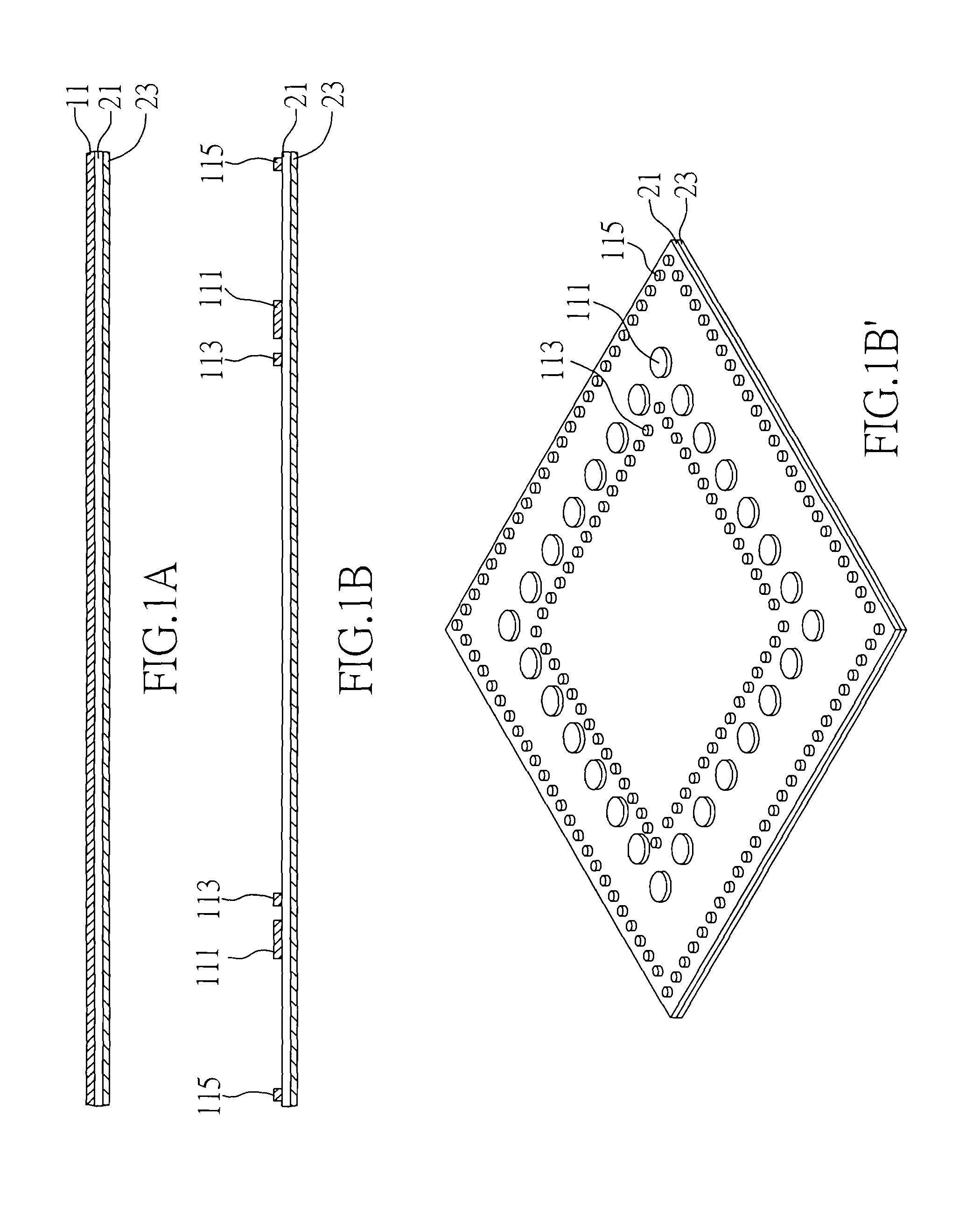
[0035]As shown in FIG. 1J, semiconductor assembly 110 includes interposer 31, stiffener 41, semiconductor chip 51, coreless substrate 20 and bond wires 321. Interposer 31 includes first surface 311, second surface 313 opposite to first surface 311, first contact pads 312 and bond fingers 316 at first surface 311, second contact pads 314 at second surface 313, conductive through-vias 318 that electrically connect portions of first contact pads 312 and second contact pads 314, and lateral routing circuitries 320 that electrically connect the bond fingers 316 and the portions of first contact pads 312. Interposer 31 can be a silicon interposer, a glass interposer or a ce...

embodiment 2

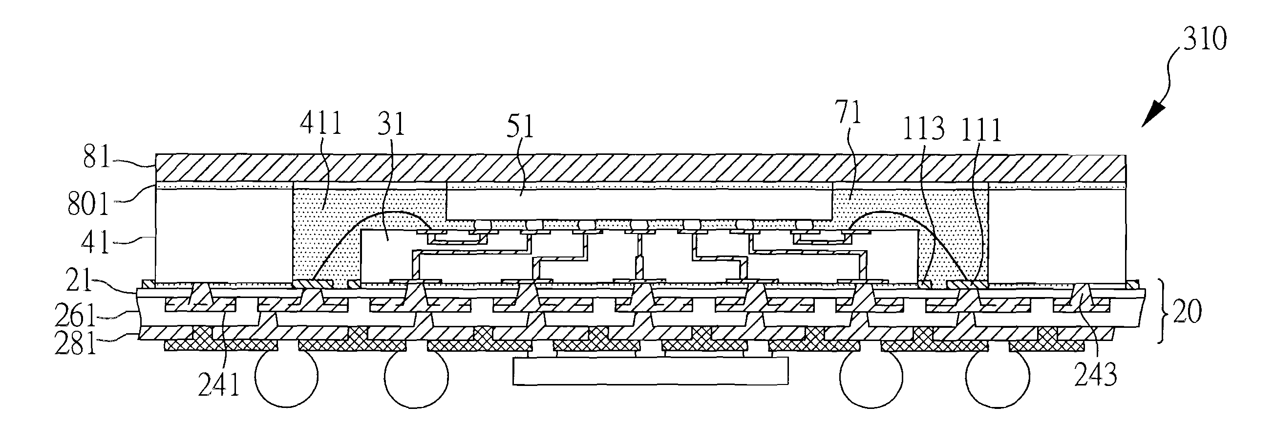
[0054]FIG. 2 is a cross-sectional view of another three dimensional assembly 310 with additional first conductive micro-vias 243 that directly contact stiffener 41 for grounding or electrical connection to passive components in accordance with another embodiment of the present invention. Also shown in FIG. 2 are encapsulant 71 and heat dissipating plate 81. Encapsulant 71 such as epoxy fills aperture 411 and covers bond pads 111, stopper 113, first dielectric layer 21, and interposer 31 in the upward direction. Heat dissipation plate 81 such as copper or aluminum is attached onto stiffener 41 and semiconductor chip 51 for assisting heat dissipation via thermally conductive adhesive 801 and covers stiffener 41, encapsulant 71 and semiconductor chip 51 in the upward direction.

[0055]The semiconductor assemblies described above are merely exemplary. Numerous other embodiments are contemplated. In addition, the embodiments described above can be mixed-and-matched with one another and wit...


PUM


Abstract

A semiconductor assembly includes a semiconductor device, a through-via interposer, a coreless substrate and a stiffener. The semiconductor device is flip mounted on the interposer, and the interposer is affixed on the coreless substrate by adhesive and extends into an aperture of a stiffener which provides mechanical support for the coreless substrate. The electrically connection between the interposer and the coreless substrate includes bond wire and conductive micro-via. The coreless substrate can provide fan-out routing for the interposer.

Description

CROSS REFERENCE TO RELATED APPLICATION[0001]This application is a continuation-in-part of U.S. application Ser. No. 13 / 615,819 filed Sep. 14, 2012 and a continuation-in-part of U.S. application Ser. No. 13 / 753,625 filed Jan. 30, 2013, each of which is incorporated by reference. U.S. application Ser. No. 13 / 753,625 filed Jan. 30, 2013 is a continuation-in-part of U.S. application Ser. No. 13 / 615,819 filed Sep. 14, 2012. U.S. application Ser. No. 13 / 615,819 filed Sep. 14, 2012 and U.S. application Ser. No. 13 / 753,625 filed Jan. 30, 2013 all claim the benefit of filing date of U.S. Provisional Application Ser. No. 61 / 682,801 filed Aug. 14, 2012.BACKGROUND OF THE INVENTION[0002]1. Field of the Invention[0003]The present invention relates to a semiconductor assembly, and more particularly to a semiconductor assembly with a semiconductor device flip mounted on an interposer which is affixed on a coreless substrate. The interposer has a through via and the interconnections between the inte...

Claims


Application Information

Patent Timeline
IPC IPC(8): H01L23/48
CPCH01L23/481H01L2224/131H01L2224/16227H01L2224/73253H01L2224/32245H01L2924/15192H01L2924/15311H01L2924/19107H01L2224/16225H01L23/16H01L23/24H01L23/3128H01L23/36H01L23/49816H01L23/49827H01L23/49833H01L21/4857H01L25/0657H01L2924/00014
Inventor LIN, CHARLES W.C.WANG, CHIA-CHUNG
Owner BRIDGE SEMICON
Why Eureka
Try Eureka