Low-voltage fast-write PMOS nvsram cell

a pmos nvsram and low-voltage technology, applied in static storage, digital storage, instruments, etc., can solve the problems of reverse polarity of stored data, corresponding sram cells need more complicated circuit handling techniques, and sram lacks permanent storage capability

Inactive Publication Date: 2014-02-20
APLUS FLASH TECH
View PDF6 Cites 25 Cited by
  • Summary
  • Abstract
  • Description
  • Claims
  • Application Information

AI Technical Summary

Benefits of technology

[0017]The fourth objective of the present PMOS NVSRAM invention is to use one of three HV PMOS transistors to isolate each input of each Flash cell from the paired Q and QB of each LV SRAM cell of each PMOS NVSRAM cell so that the boosting negative HV within the PMOS Flash channel during the SBPI Program operation would not be coupled to any P / N junction of each LV SRAM cell to avoid junction breakdown.
[0018]The fifth objective of the present PMOS NVSRAM cell invention is to provide one preferred set of Erase and Erase-Inhibit bias conditions by coupling the PMOS Flash gate voltage, FWL, with a positive high voltage (HV) along with coupling the PMOS Flash cell's Source and Drain nodes as well its N-well node to 0V. As a result, the electrons in the Flash channel would be injected into the poly1 floating-gate, allowing for the low-current channel FN tunneling effect on both two PMOS Flash cells in the two 3 T PMOS Flash strings.

Problems solved by technology

But the SRAM lacks of permanent storage capability after the normal power off or the unexpected power loss.
Although the NMOS NVSRAM cells have many advantages, there is one severe drawback which is the reverse of the polarity of stored data between each SRAM and each Flash cell in each NVSRAM cell after program operation of each NMOS NVSRAM.
As a result, during the power-up period, the downloading of each Flash data into each corresponding SRAM cell needs more complicate circuit handling technique to make it into the same data polarity.

Method used


Image

  • Low-voltage fast-write PMOS nvsram cell
  • Low-voltage fast-write PMOS nvsram cell
  • Low-voltage fast-write PMOS nvsram cell

Examples


Embodiment Construction

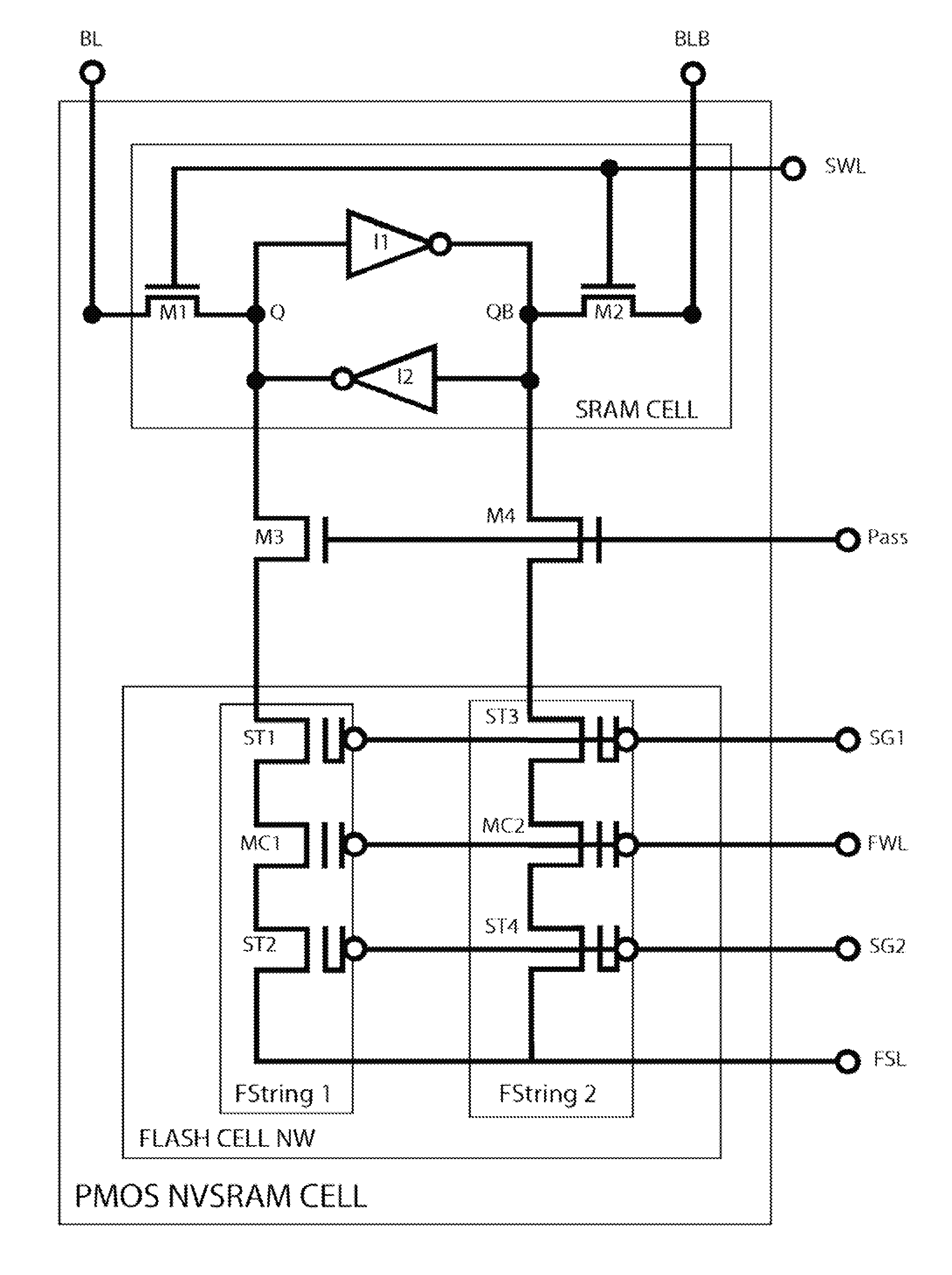
[0045]The present invention is generally related with a novel design of PMOS SRAM based NVRAM cell structure and array for an extremely fast Write (program and erase) speed but with only requires the low-voltage VDD and VSS for Program and Program-Inhibit operation for an extremely high-density, low-current, in-circuit programmable and erasable NVSRAM and SRAM-based FPGA designs. More particularly, unlike the previous NMOS NVSRAM cells invented by the same inventors and others, this preferred PMOS NVSRAM cell structure can be used extensively to those applications of SRAM-based FPGA IC design with a fast 10 ms simultaneously chip write on an extremely high memory density of up to 1 Gb at a low VDD read operation down to 1.2V.

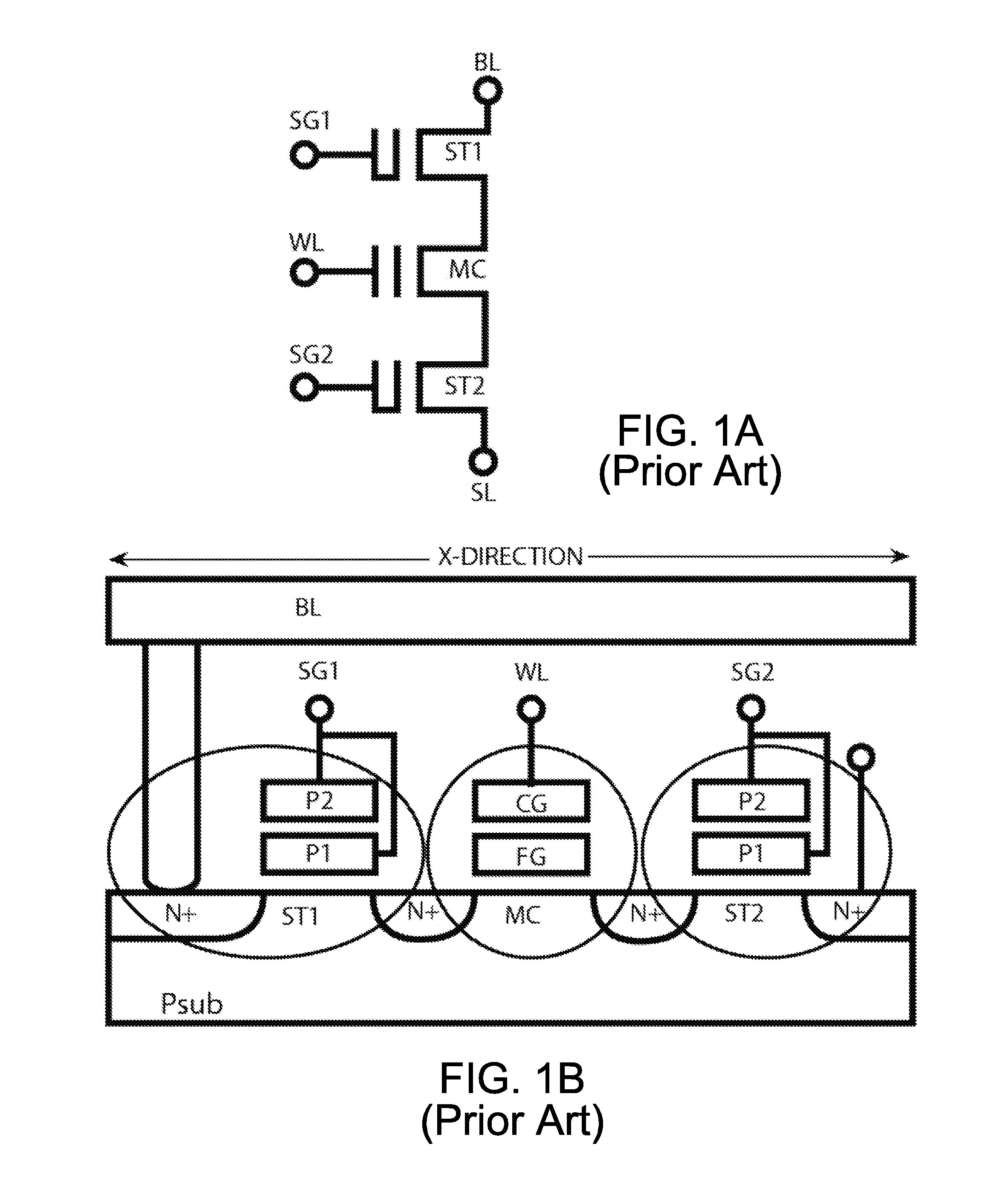
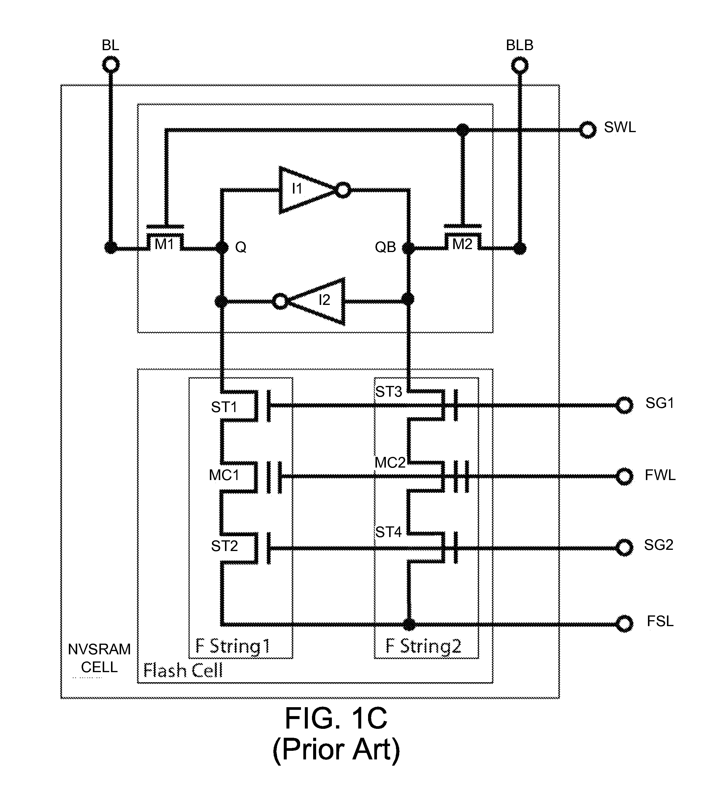
[0046]To better illustrate the preferred PMOS NVSRAM cell, a revisit of some structures NVSRAM cells presented in prior art would be helpful. FIG. 1A is a schematic diagram of a 3 T NMOS Flash string used in a NMOS NVSRAM cell of prior art. Presenting this tradi...


PUM


Abstract

This invention discloses a low-voltage fast-write 12T or 14T PMOS NVSRAM cell structure which comprises a 6T LV SRAM cell and one pairs of two 3T or 4T HV PMOS Flash strings. Due to reverse threshold voltage definition of PMOS and NMOS flash cell, this PMOS NVSRAM cell has the advantage over the NMOS NVSRAM cell to have the same data polarity between SRAM and Flash pairs during the data writing operation. In addition, this PMOS NVSRAM's PMOS Flash cell uses similar low-current FN-tunneling scheme as NMOS NVSRAM, thus the fast data program and erase can be achieved in a big density up to 100 Mb simultaneously. As a result, low power voltage operation of NVSRAM with 1.2V VDD can be much easier to be designed without coupling the FSL line to any VDD level during the flash data loading into SRAM cell during a power-on period.

Description

CROSS-REFERENCES TO RELATED APPLICATIONS[0001]This application claims priority to U.S. Provisional Patent Application No. 61 / 742,683, filed on Aug. 15, 2012, commonly assigned, and hereby incorporated by reference in its entirety herein for all purposes.[0002]This application is related to U.S. Pat. Nos. 8,018,768, 7,760,540, 7,110,293, and 7,859,899.BACKGROUND OF THE INVENTION[0003]The present invention is generally related with a novel design of PMOS SRAM based NVRAM cell structure and array for an extremely fast Write (Program and Erase) speed, which only requires the low-voltage VDD and VSS for Program and Program-Inhibit operations for an extremely high-density, low-current, in-circuit programmable and erasable NVSRAM and SRAM-based field-programmable gate array (FPGA) designs.[0004]The CMOS NVSRAM is well known for years in the art. Typically, it comprises a 6 T SRAM cell and a Flash cell. During the read operation, Flash is isolated from SRAM and is transparent to the SRAM us...

Claims


Application Information

Patent Timeline
Patent Type & Authority Applications(United States)
IPC IPC(8): G11C14/00
CPCG11C14/0063G11C14/00G11C16/04G11C16/0433G11C16/16
Inventor TSAO, HSING-YALEE, PETER WUNG
Owner APLUS FLASH TECH
Why Eureka
Try Eureka