

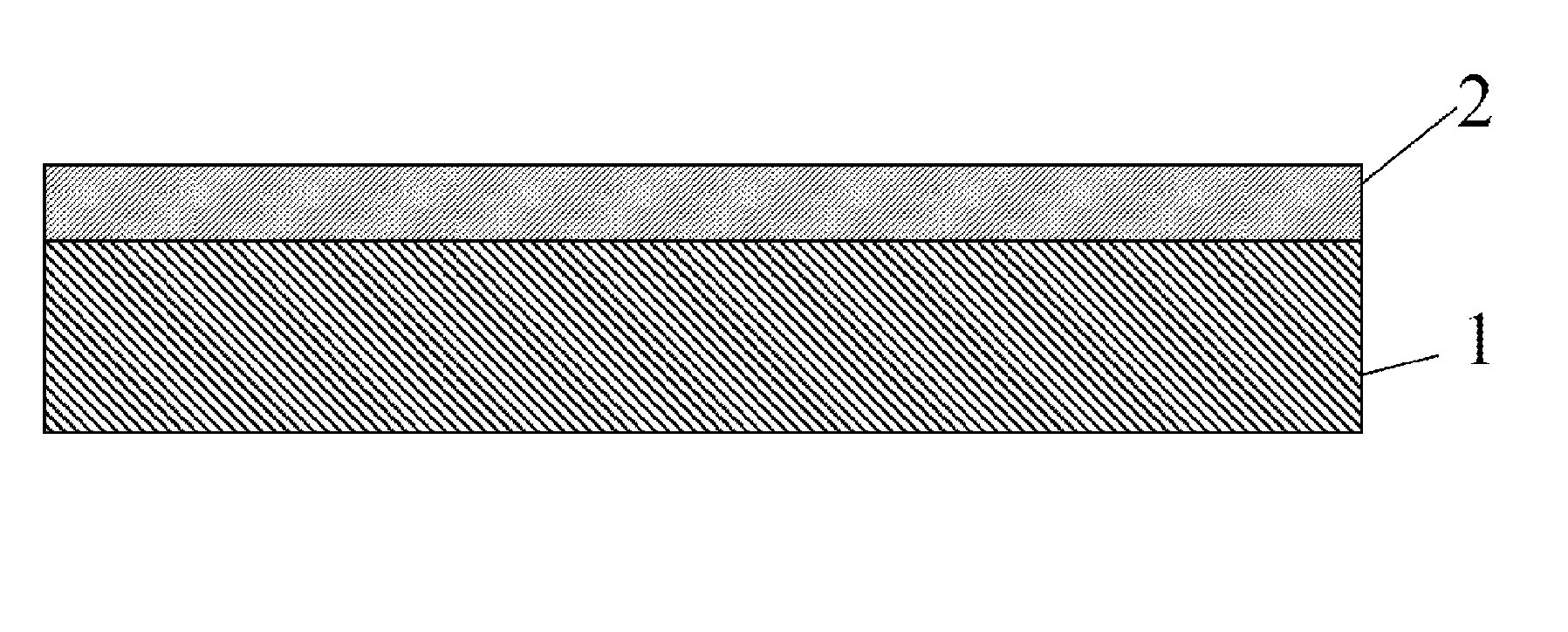
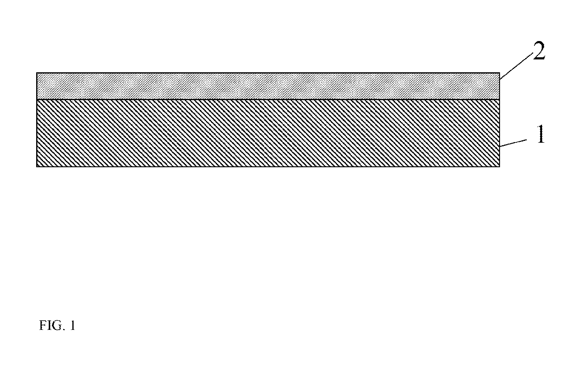
Composite substrate of gallium nitride and metal oxide
a technology of metal oxide and composite substrate, which is applied in the direction of semiconductor devices, semiconductor/solid-state device testing/measurement, electrical apparatus, etc., can solve the problems of difficult to grow gan crystal ingots, high cost of gan substrates, and hinder the realization of high-end optical and electronic devices
- Summary
- Abstract
- Description
- Claims
- Application Information
AI Technical Summary
Benefits of technology
Problems solved by technology
Method used
Image

Examples
example 1
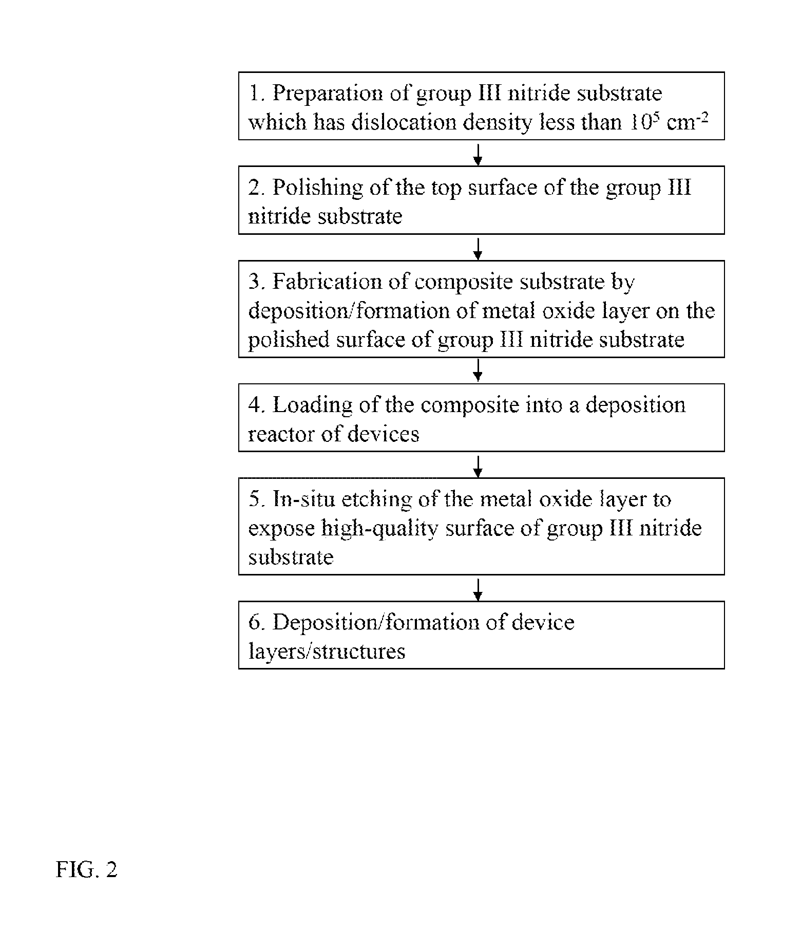
[0032]Zinc oxide layer can be deposited on the Ga-polar surface of c-plane GaN substrate having dislocation density less than 105 cm−2 with hydrothermal deposition at 300° C. The thickness of the first layer can be about 300 microns and the thickness of the second layer can be 1 micron. The zinc oxide layer can be etched under ammonia flow in the MOCVD reactor while ramping the substrate temperature. If the ramp time is not long enough to remove all zinc oxide layer, the substrate is maintained at about 1050° C. under ammonia ambient until the GaN layer is exposed. This way, the interface between the GaN substrate and the device layer can be smooth and generation of new dislocations can be avoided.
example 2
[0033]Silicon oxide layer can be deposited on the Ga-polar surface of c-plane GaN substrate having dislocation density less than 105 cm−2 with a spin-coat technique. The spin-coated composite substrate is baked at about 150° C. The thickness of the first layer can be about 300 microns and the thickness of the second layer can be 10 microns. If the silicon oxide layer is formed at low temperature, the layer can be etched under ammonia flow in the MOCVD reactor while ramping the substrate temperature. If the ramp time is not long enough to remove all silicon oxide layer, the substrate is maintained at about 1050° C. under ammonia ambient until the GaN layer is exposed. This way, the interface between the GaN substrate and the device layer can be smooth and generation of new dislocations can be avoided.
example 3
[0034]Gallium oxide layer can be formed on the Ga-polar surface of c-plane GaN substrate having dislocation density less than 105 cm−2 with acid etching. The thickness of the first layer can be about 300 microns and the thickness of the second layer can be a few monolayers. The gallium oxide layer can be etched under ammonia flow in the MOCVD reactor while ramping the substrate temperature. If the ramp time is not long enough to remove all gallium oxide layer, the substrate is maintained at about 1050° C. under ammonia ambient until the GaN layer is exposed. This way, the interface between the GaN substrate and the device layer can be smooth and generation of new dislocations can be avoided.
PUM
| Property | Measurement | Unit |
|---|---|---|
| diameter | aaaaa | aaaaa |
| temperature | aaaaa | aaaaa |
| temperature | aaaaa | aaaaa |
Abstract
Description
Claims
Application Information