Supercharge Your Innovation With Domain-Expert AI Agents!

Tft-lcd array substrate

a technology of array substrate and thin film transistor, which is applied in the direction of identification means, instruments, semiconductor devices, etc., can solve the problems of poor process tolerance, weakening the competitiveness of manufacturers, and weakening the quality of 4mask technology, so as to improve the ratio of acceptable products and reduce production costs

Inactive Publication Date: 2014-03-13
BEIJING BOE OPTOELECTRONCIS TECH CO LTD
View PDF3 Cites 4 Cited by
  • Summary
  • Abstract
  • Description
  • Claims
  • Application Information

AI Technical Summary

Benefits of technology

The present invention provides a TFT-LCD array substrate with a repairable pixel structure to improve the ratio of acceptable products and reduce production cost. A spare TFT is provided alongside the primary TFT, which allows the defective channel region to be cut off and the spare drain electrode and pixel electrode to be directly connected by laser to repair the defective pixel. This improves the ratio of acceptable products and high-class products and further reduces the production cost.

Problems solved by technology

With expansion of the production of thin film transistor liquid crystal displays (TFT-LCDs), competition among manufacturers becomes severer.
However, the 4Mask technology has its inherent drawbacks.
This not only results in a poor process tolerance, but also makes the production conditions complicated and difficult to control.
Among the defects in the TFT-LCD array substrate produced by the 4Mask technology, an open circuit in the active layer and a short circuit of the source / drain electrode in the channel region of the pixel TFT occur most frequently, which mainly result from the characteristic of the 4Mask technology.
However, the repair in this way reduces the yield of the TFT-LCD.

Method used


Image

  • Tft-lcd array substrate
  • Tft-lcd array substrate
  • Tft-lcd array substrate

Examples


Embodiment Construction

[0018]The present invention is to form a spare TFT alongside a conventional TFT. When a source electrode, a drain electrode and a channel region of a primary TFT are formed with a gray tone mask, a spare source electrode, a spare drain electrode, and a spare channel region are formed alongside the channel region of the primary TFT so as to form a spare TFT. The source electrode of the spare TFT is connected with or formed as a part of the source electrode of the primary TFT, and the drain electrode is arranged under the pixel electrode.

[0019]Hereinafter, the present invention will be described in detail with reference to the drawings.

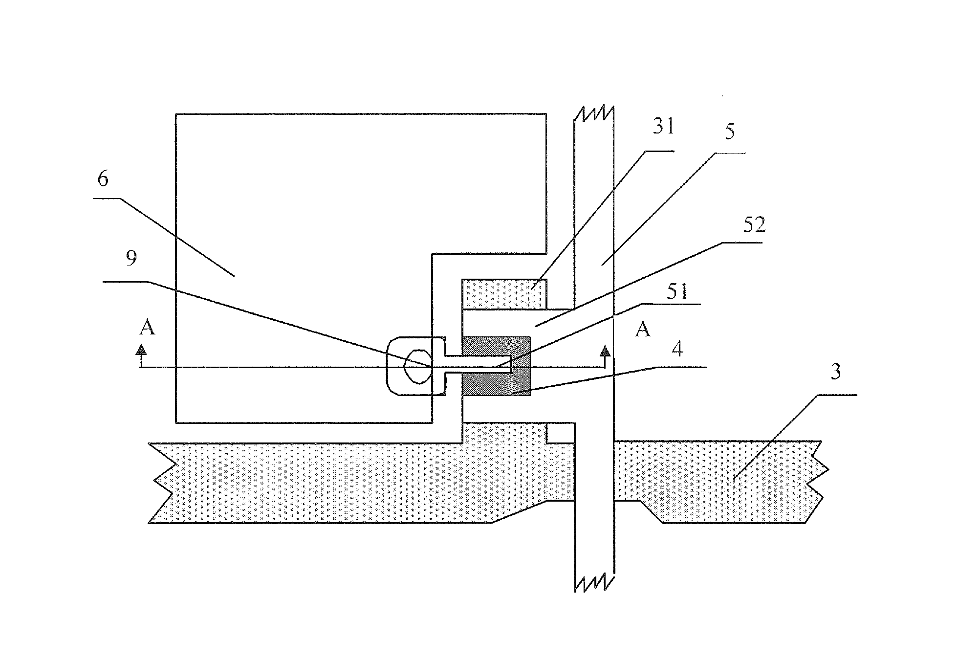
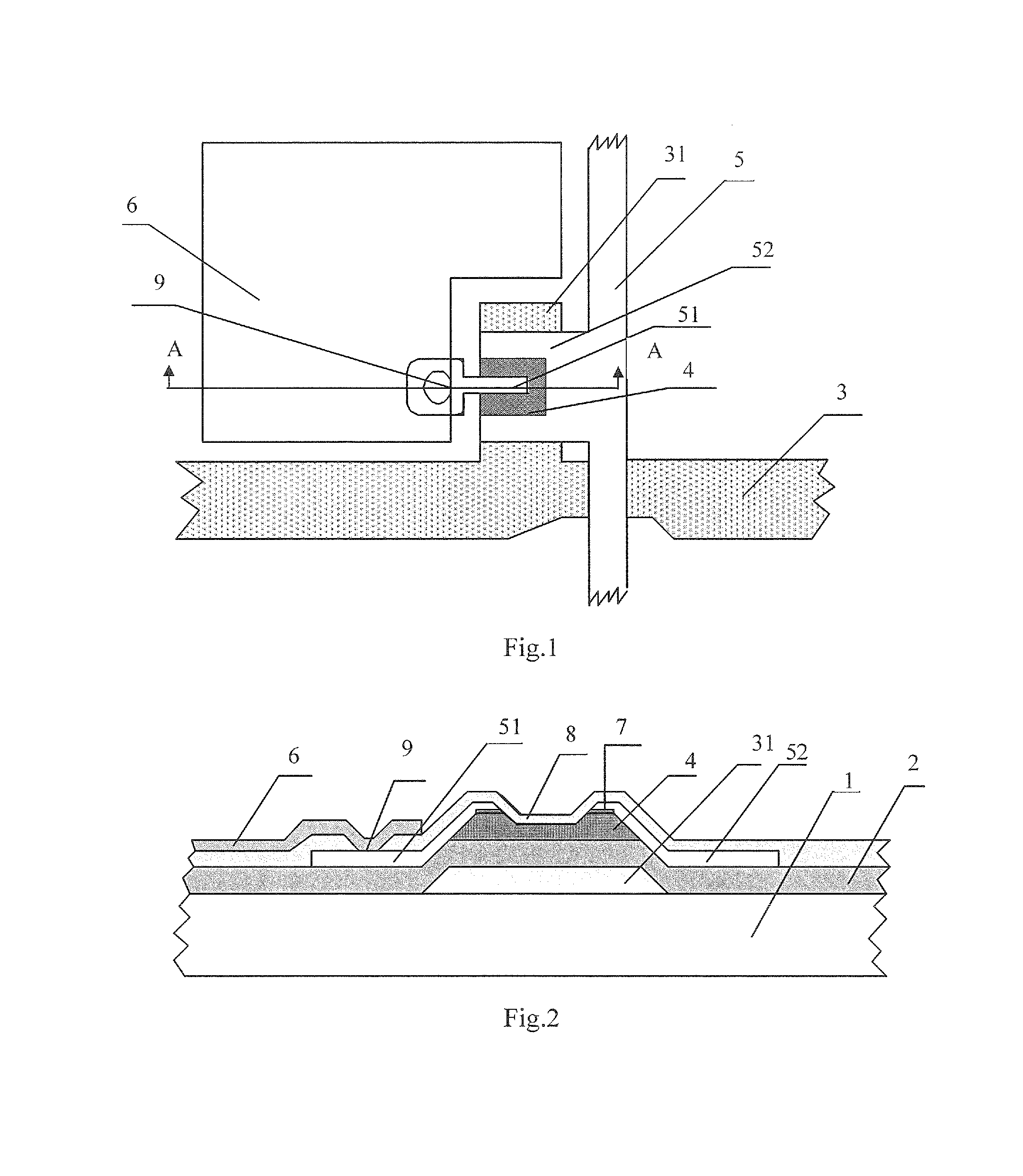
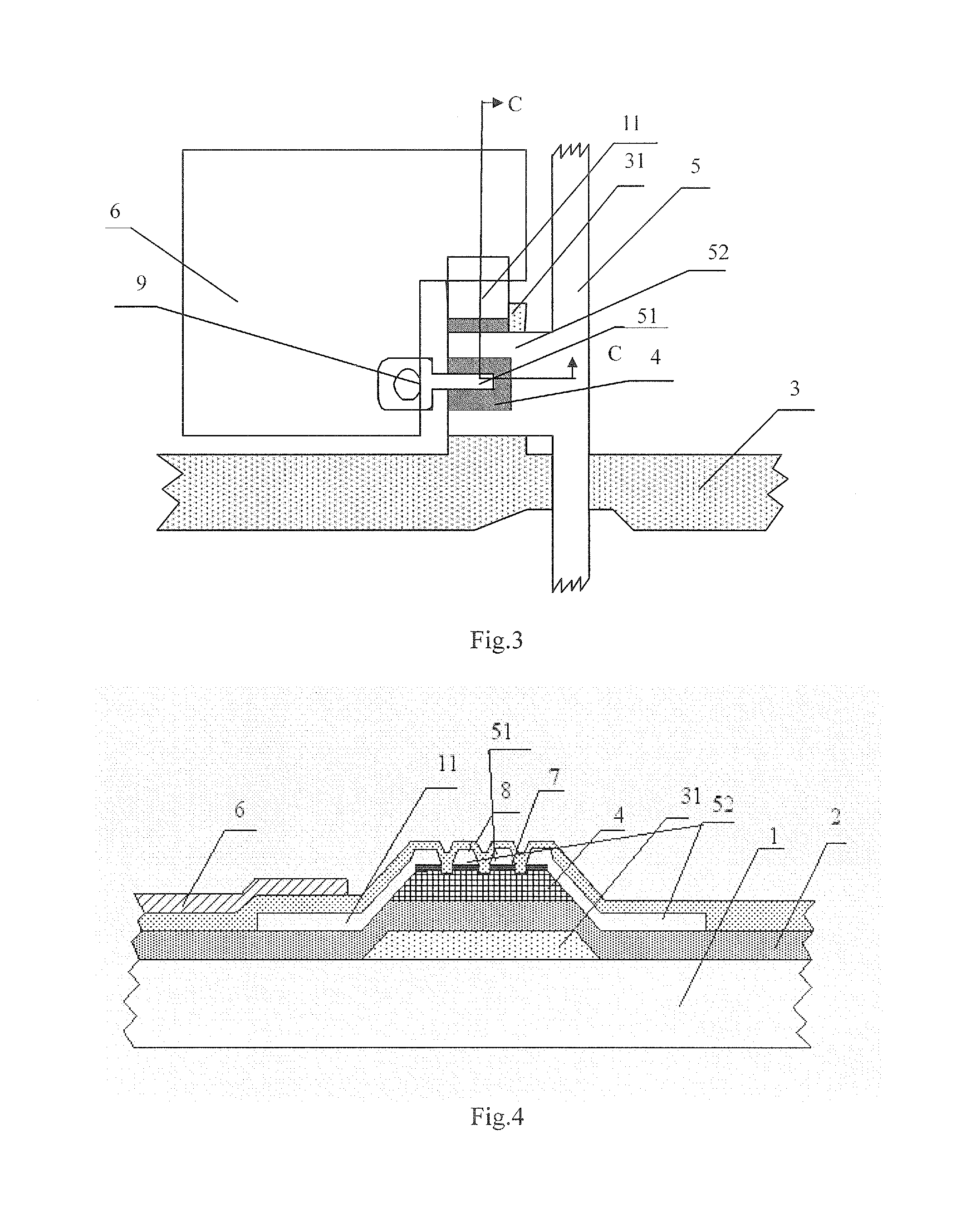
[0020]FIG. 3 is a schematic diagram showing a pixel structure according to an embodiment of the present invention, and FIG. 4 is a cross-sectional view taken along the line C-C in FIG. 3.

[0021]As shown in FIGS. 3 and 4, according to the embodiment of the present invention, the pixel structure comprises a glass substrate 1 and a gate line 3 and data line...


PUM

PropertyMeasurementUnit
transparentaaaaaaaaaa
timeaaaaaaaaaa
shapeaaaaaaaaaa

Abstract

A thin film transistor liquid crystal display (TFT-LCD) array substrate with a repairable pixel structure is provided. The array substrate comprises a gate line and a data line, and the gate line and the data line intersect with each other to define a pixel unit. The pixel unit comprises a TFT and a pixel electrode, and a spare source electrode, a spare drain electrode, and a spare channel region are formed alongside a channel region of the TFT to form a spare TFT.

Description

FIELD OF THE INVENTION[0001]The present invention relates to a thin film transistor-liquid crystal display (TFT-LCD) array substrate, and particularly, to a TFT-LCD array substrate with a repairable pixel structure.BACKGROUND OF THE INVENTION[0002]With expansion of the production of thin film transistor liquid crystal displays (TFT-LCDs), competition among manufacturers becomes severer. The manufacturers have been not only continuously improving the performance of the products but also decreasing the production cost of the products, so as to enhance their competitive power in the market. To decrease the production cost, most of the manufacturers have focus their efforts on reducing the number of processes (especially the number of photolithography processes), thus decreasing the production period and production cost.[0003]In recent years, the number of photolithography processes in the manufacturing process of a TFT-LCD has been decreasing. The manufacturing technology for a TFT-LCD...

Claims


Application Information

Patent Timeline
Patent Type & Authority Applications(United States)
IPC IPC(8): G02F1/1362G02F1/1368G09F9/30H01L21/336H01L29/786
CPCG02F1/136286G02F1/136259H01L27/124G02F1/136236G02F1/136231G02F1/136268G02F1/136
Inventor ZHAO, JIGANGKIM, KI YONGXU, YUBO
Owner BEIJING BOE OPTOELECTRONCIS TECH CO LTD
Features
  • R&D
  • Intellectual Property
  • Life Sciences
  • Materials
  • Tech Scout
  • Unparalleled Data Quality
  • Higher Quality Content
  • 60% Fewer Hallucinations
Learn More