Semiconductor device having buried layer and method for forming the same

a technology of semiconductor devices and layers, applied in the direction of semiconductor devices, semiconductor/solid-state device details, electrical equipment, etc., can solve the problem of increasing the manufacturing cost of ic devices

Active Publication Date: 2014-03-20
SEMICON MFG INT (SHANGHAI) CORP
View PDF5 Cites 15 Cited by
  • Summary
  • Abstract
  • Description
  • Claims
  • Application Information

AI Technical Summary

Benefits of technology

[0007]According to various embodiments, there is provided a method for forming a buried layer by providing a hard mask layer on a semiconductor substrate. The hard mask layer can have a plurality of through-openings. A plurality of deep trenches can be formed in the semiconductor substrate usin...

Problems solved by technology

However, due to high manufacturing cost of the epitaxia...

Method used


Image

  • Semiconductor device having buried layer and method for forming the same
  • Semiconductor device having buried layer and method for forming the same
  • Semiconductor device having buried layer and method for forming the same

Examples


Embodiment Construction

[0013]Reference will now be made in detail to exemplary embodiments of the disclosure, which are illustrated in the accompanying drawings. Wherever possible, the same reference numbers will be used throughout the drawings to refer to the same or like parts.

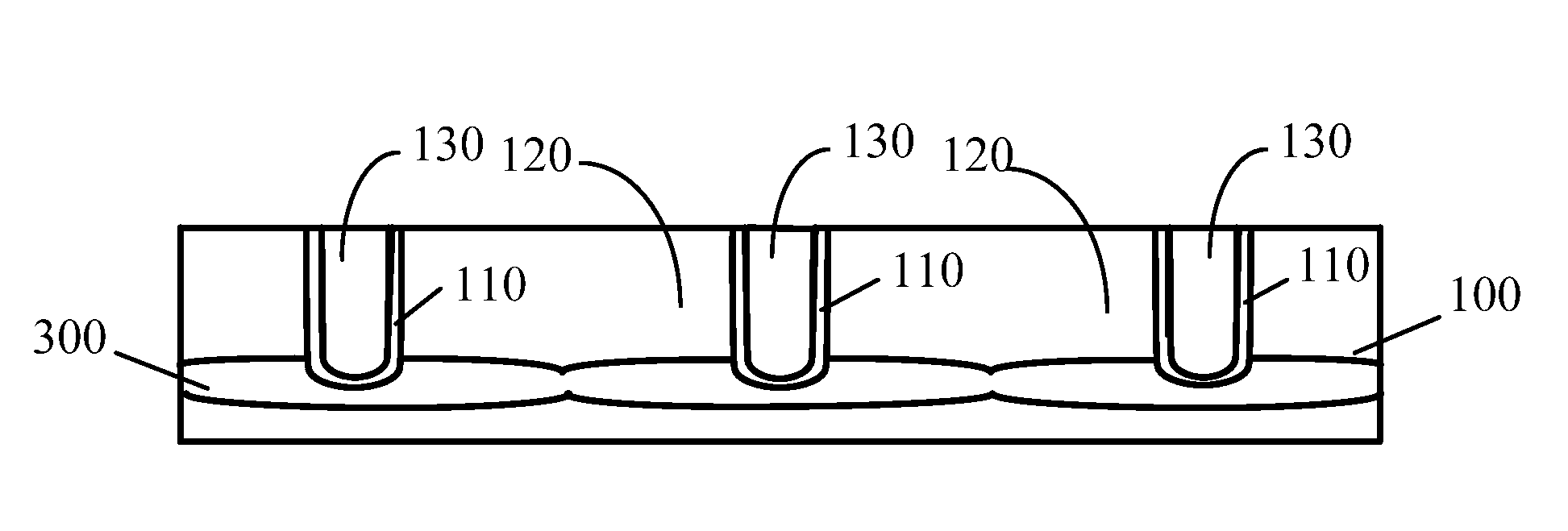
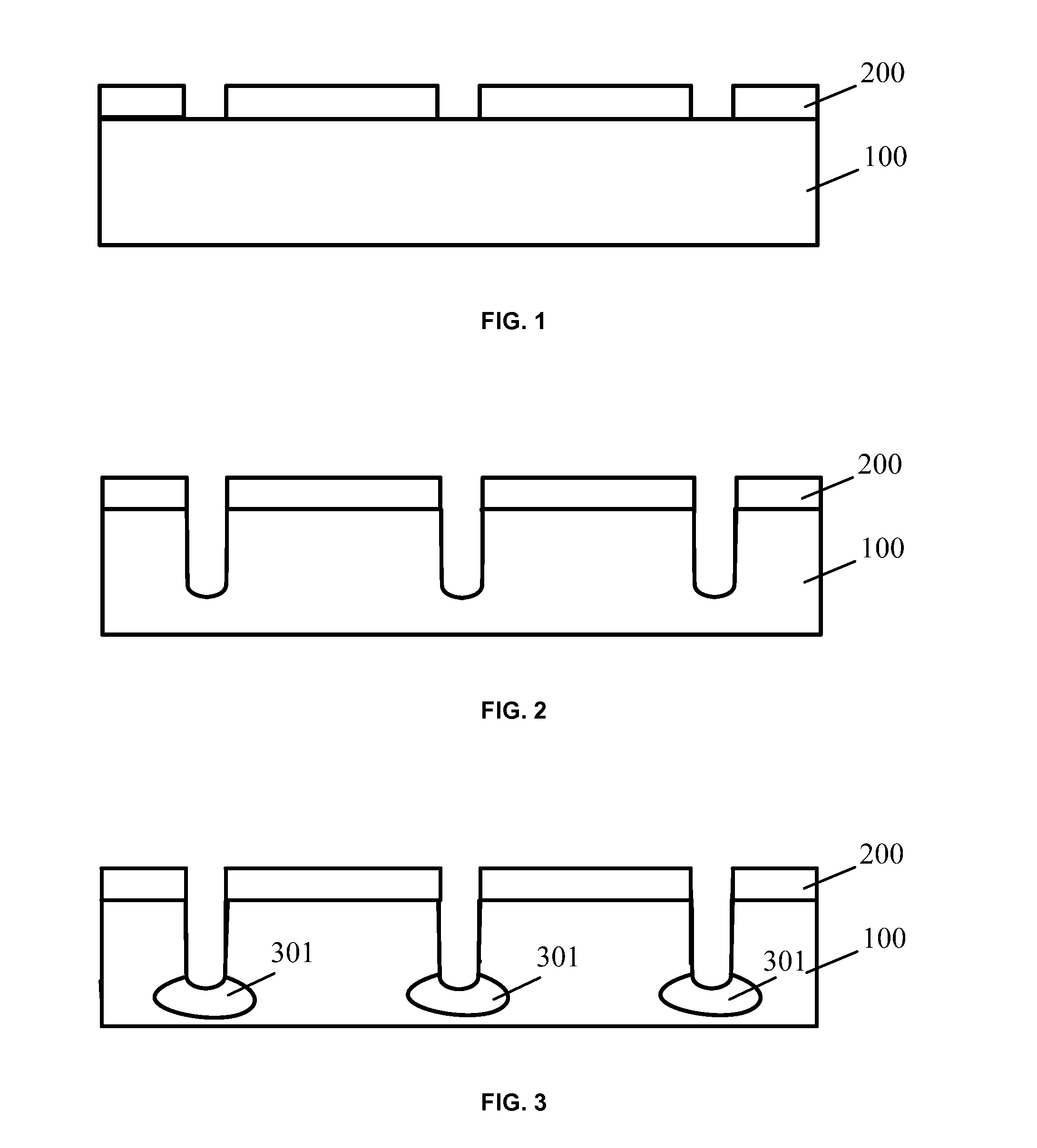
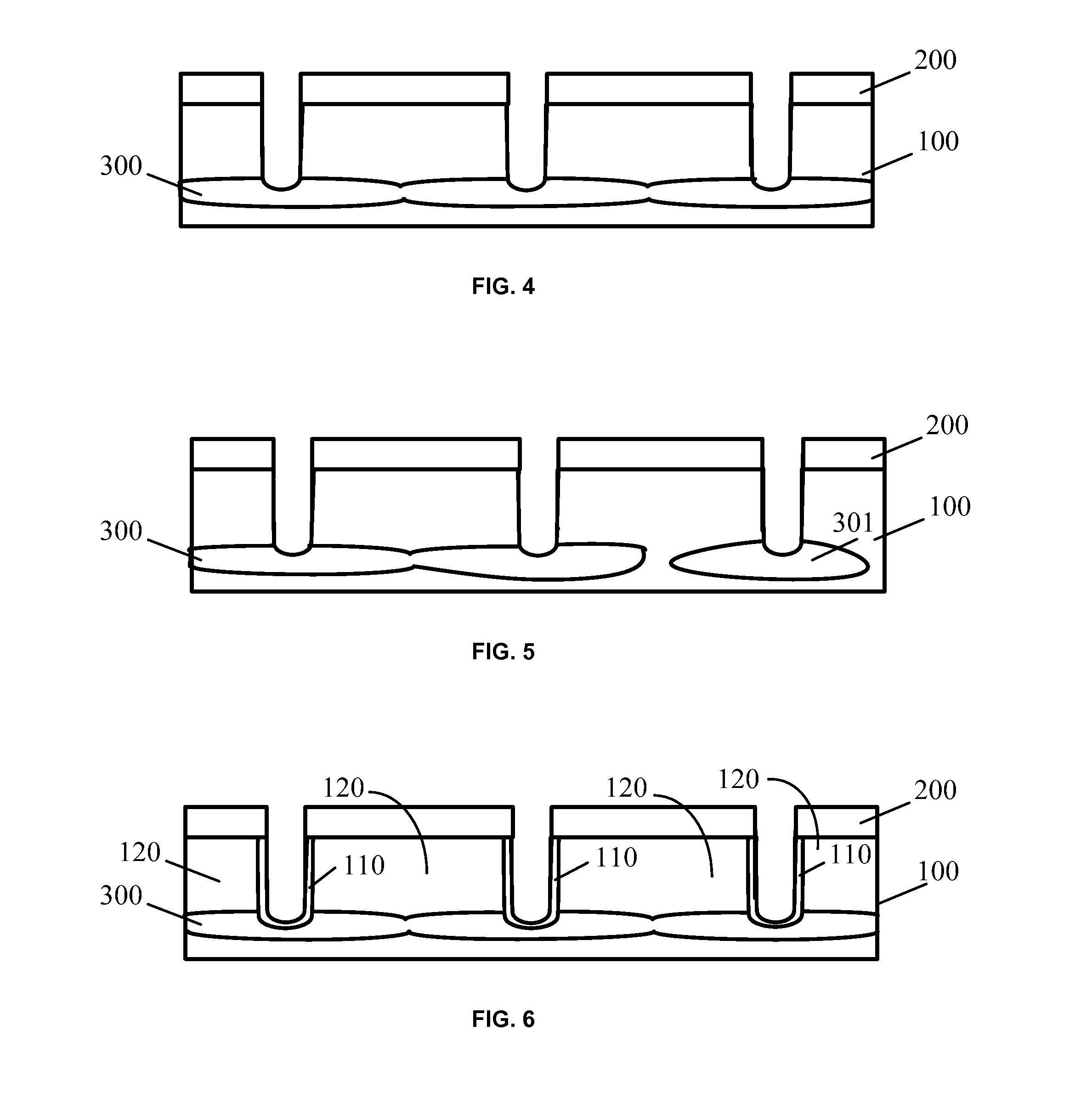
[0014]When forming a buried layer, an epitaxial layer needs to be formed on a substrate after formation of the buried layer. Such epitaxial process has relatively high manufacturing cost with more process steps. To reduce the cost of IC manufacturing and number of process steps, a method for forming a buried layer is provided. In this method, a plurality of deep trenches can be formed in a substrate. The bottom of the plurality of deep trenches can be heavily ion doped. After performing drive-in process of a plurality of heavily-doped regions, the plurality of heavily-doped regions can be laterally connected to form a buried layer.

[0015]According to different substrate types, appropriate dopant ions can be selected. For example, d...


PUM


Abstract

Semiconductor devices having a buried layer and methods for forming the same are disclosed. In an exemplary method, a hard mask layer can be provided on a semiconductor substrate. The hard mask layer can have a plurality of through-openings. A plurality of deep trenches can be formed in the semiconductor substrate using the hard mask layer as a mask. A bottom of each of the plurality of deep trenches in the semiconductor substrate can be doped to form a plurality of heavily-doped regions. One or more of the plurality of heavily-doped regions can be connected to form the buried layer in the semiconductor substrate. There is thus no need to use an epitaxial process to form active regions. In addition, lateral isolation structures can be simultaneously formed in the semiconductor substrate.

Description

CROSS-REFERENCES TO RELATED APPLICATIONS[0001]This application claims priority to Chinese Patent Application No. CN201210349799.6, filed on Sep. 18, 2012, the entire contents of which are incorporated herein by reference.FIELD OF THE DISCLOSURE[0002]The present disclosure relates to the field of semiconductor technology and, more particularly, relates to semiconductor devices having a buried layer and methods for forming the same.BACKGROUND[0003]Semiconductor buried layers are widely used in integrated circuit (IC) devices and manufacturing processes. Particularly, semiconductor buried layers are widely used in semiconductor devices including transistors, diodes, and metal-oxide-semiconductor (MOS) transistors in IC processes that require high performance. Development of the buried layer technology greatly affects IC performance and IC manufacturing process development.[0004]Buried layer technology may reduce on-resistance of the IC devices and may improve degree of integration and ...

Claims


Application Information

Patent Timeline
IPC IPC(8): H01L29/06
CPCH01L29/0623H01L21/74H01L21/2253H01L21/76213H01L21/76224H01L29/0821H01L29/732H01L21/18H01L29/73
Inventor HE, JIWEIWANG, GANGNINGPU, SHANNONTANG, MIKEFENG, AMY
Owner SEMICON MFG INT (SHANGHAI) CORP
Why Eureka
Try Eureka