

Dual shallow trench isolation liner for preventing electrical shorts
a technology of shallow trenches and isolation lines, applied in the field of semiconductoroninsulators, can solve the problems of severe yield problems and erosion of shallow trench isolation structures, and achieve the effect of sufficient electrical isolation
- Summary
- Abstract
- Description
- Claims
- Application Information
AI Technical Summary
Benefits of technology
Problems solved by technology
Method used
Image


Examples
first embodiment
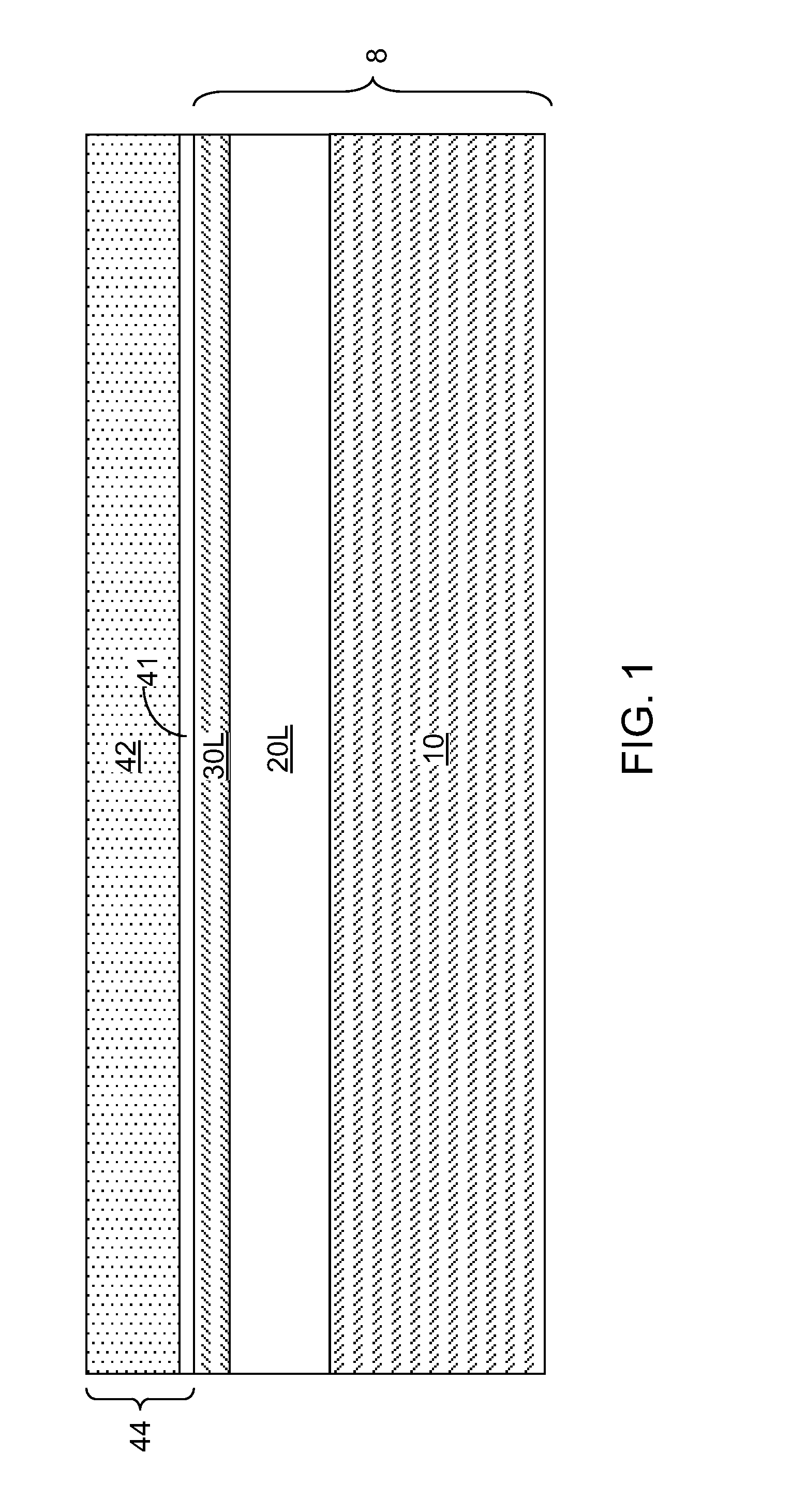
[0033]Referring to FIG. 1, a first exemplary semiconductor structure according to the present disclosure includes a semiconductor-on-insulator (SOI) substrate 8. The SOI substrate 8 includes a vertical stack of a handle substrate 10, a buried insulator layer 20L, and a top semiconductor layer 30L.
[0034]The handle substrate 10 can include a semiconductor material, a dielectric material, a conductive material, or a combination thereof. For example, the handle substrate 10 can be a single crystalline silicon substrate. The buried insulator layer 20L includes a dielectric material such as silicon oxide, silicon nitride, silicon oxynitride, or a combination thereof. The top semiconductor layer 30L includes a semiconductor material such as silicon, germanium, a silicon-germanium alloy, a III-V compound semiconductor, a II-VI compound semiconductor, any other semiconductor material known in the art, or combinations thereof. The semiconductor material in the top semiconductor layer 30L can ...
second embodiment
[0068]Referring to FIG. 17, a second exemplary semiconductor structure according to the present disclosure can be derived from the first exemplary semiconductor structure of FIG. 15 by depositing a contact-level silicon nitride layer 90 as another contact-level dielectric material layer prior to depositing the contact-level dielectric material layer 91. In this case, the etch process employed to form the various contact via holes (82, 84, 86) includes a silicon nitride etch that transfers the pattern of the openings in the photoresist 97 through the contact-level silicon nitride liner 90.
[0069]The silicon nitride etch is not selective to the silicon nitride material of the silicon nitride liner 48, and consequently, the silicon nitride liner 48 can be recessed below the horizontal plane of the bottom surface of the top semiconductor portion 30, and in some cases, below the horizontal plane of the bottom surface of the buried insulator portion 20. Further, if the dielectric material ...
PUM
 Abstract
Description
Claims
Application Information