Active-matrix Panel Display Device, TFT and Method for Forming the Same

a technology of active matrix and display device, which is applied in the field of display technology, can solve the problems of deterioration in properties and instability of oxide tft, and achieve the effect of ensuring stability of tft and display quality of active matrix display devi

Inactive Publication Date: 2014-05-01
SHENZHEN CHINA STAR OPTOELECTRONICS TECH CO LTD
View PDF8 Cites 2 Cited by
  • Summary
  • Abstract
  • Description
  • Claims
  • Application Information

AI Technical Summary

Benefits of technology

[0022]In contrast to prior art, the beneficial effect of the present invention is that the present invention stacks an oxide semiconductor layer and a buffer layer in order on a first insulating layer and respectively forms a source and a drain on the oxide semiconductor layer and the buffer layer. The buffer layer which does not directly contact the source and the drain is applied to plasma process or heating process in oxygen atmosphere so

Problems solved by technology

The oxide semiconductor of the BCE Oxide TFT however, is easily damaged by follow-up processes, e.g. etching a sour

Method used


Image

  • Active-matrix Panel Display Device, TFT and Method for Forming the Same
  • Active-matrix Panel Display Device, TFT and Method for Forming the Same
  • Active-matrix Panel Display Device, TFT and Method for Forming the Same

Examples


first embodiment

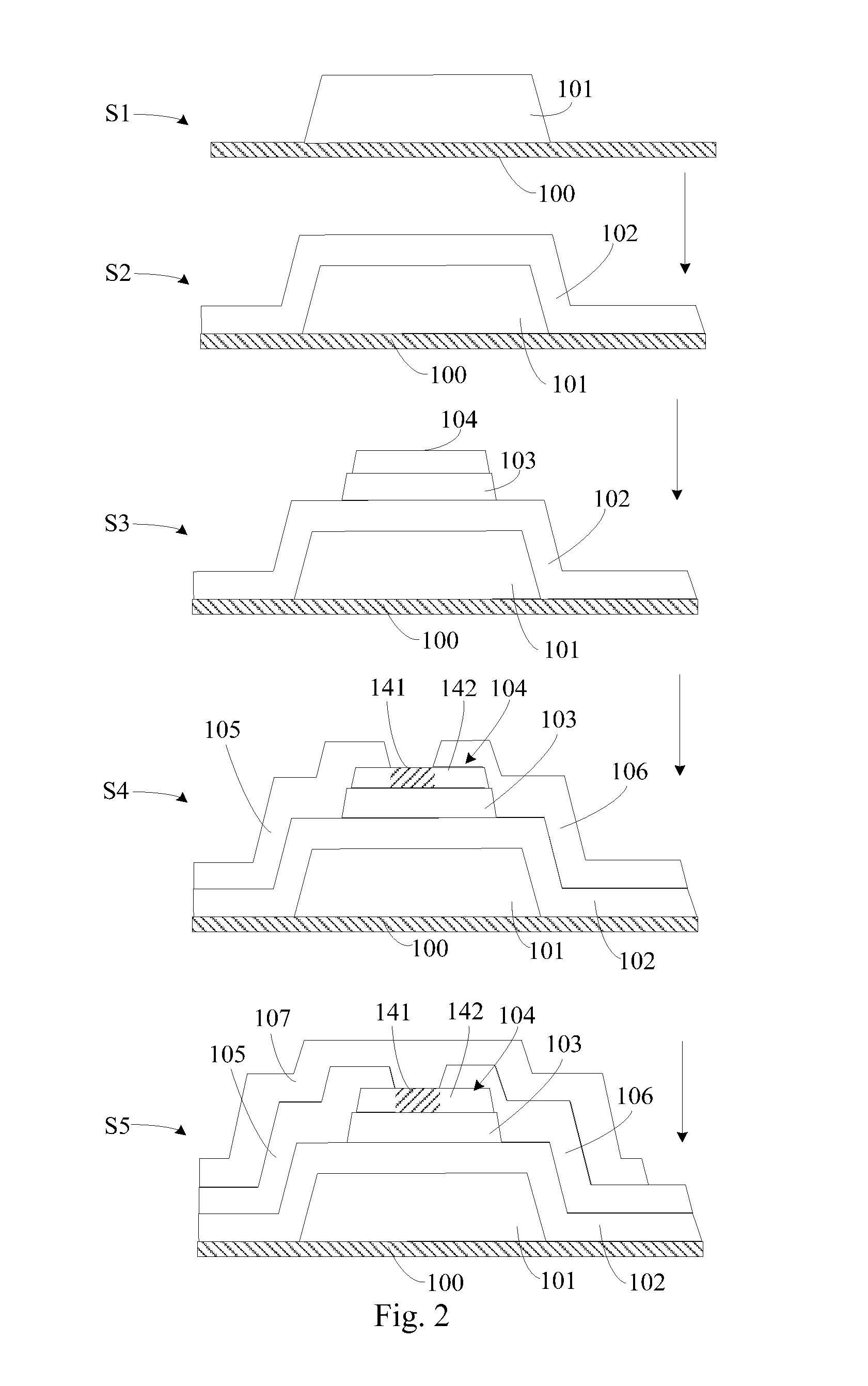
[0030]Please refer to FIG. 1 in conjunction with FIG. 2. FIG. 1 is a flowchart of a method for forming a TFT according to the present invention, and FIG. 2 is a process diagram corresponding to the method for forming the TFT in FIG. 1. The method of forming the TFT composes the following steps:

[0031]Step S1: Form a gate 101 on a substrate 100;

[0032]the substrate 100 is provided and the gate 101 is arranged on the substrate 100. The gate 101 as a control electrode of a TFT is used for controlling on / off states of the TFT in response to an external signal.

[0033]Step S2: Form a first insulating layer 102 on the gate 101;

[0034]the first insulating layer 102 formed on the gate is used for insulating the gate 101 from other layers.

[0035]Step S3: Stack an oxide semiconductor layer 103 and a buffer layer 104 on the first insulating layer 102 in order;

[0036]the oxide semiconductor layer 103 is formed on the first insulating layer 102 and the buffer layer 104 is formed on the oxide semiconduc...

second embodiment

[0045]Please refer to FIG. 3. FIG. 3 illustrates a structure diagram of a TFT according to the present invention. As FIG. 3 shows, a TFT 300 comprises to gate 301, a first insulating layer 302, an oxide semiconductor layer 303, a buffer layer 304, a source 305, a drain 306, and a second insulating layer 307.

[0046]The first insulating layer 302 on the gate 301 is a gate insulating layer. The oxide semiconductor layer 303 and the buffer layer 304 stack in order on the first insulating layer 301. The oxide semiconductor layer 303 is close to the first insulating layer 302, and the buffer layer 304 is on the oxide semiconductor layer 303. The buffer layer 304 comprises a butler layer 341 which does not contact the source 305 and the drain 306 directly and a buffer layer 342 which contacts the source 305 and the drain 306 directly. The stack of the buffer layer 304 and the oxide semiconductor layer 303 is formed by sputtering thin films and etching the thin films by oxalic acid at the sa...

third embodiment

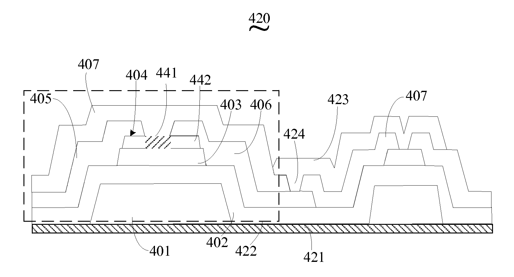
[0051]Referring to FIG. 4, FIG. 4 is a structure diagram of an active-matrix panel display device according to the present invention. As FIG. 4 shows, an active-matrix panel display device 400 comprises a color filter substrate 410 and an array substrate 420 set up relatively.

[0052]The array substrate 420 comprises a substrate 421. Preferably, material of the substrate 421 is glass. By coating and etching processes, the main elements, such as scan lines, data lines, pixel electrodes and TFTs, are formed on the substrate 421.

[0053]Please refer to FIG. 5, FIG. 5 is a structure diagram of the array substrate 420 in the active-matrix panel display device in FIG. 4. As FIG. 5 shows, the array substrate 420 comprises the substrate 421, a TFT 422 and a transparent conducting layer 423. The structure of the TFT 422 is the same with that of the TFT 300 in FIG. 3.

[0054]In the embodiment, the transparent conducting layer 423 as a pixel electrode of the array substrate 420 is on the second insu...


PUM


Abstract

The present invention discloses an active-matrix panel display device, a TFT and a method for forming the same The method includes that arranging a first insulating layer on a gate, stacking an oxide semiconductor layer and a buffer layer in order on the first insulating layer, arranging as source on the oxide semiconductor layer and a drain on the buffer layer, and plasma processing or heating in oxygen atmosphere the buffer layer which does not directly contact the source and the drain. Therefore, the present invention is capable of preventing the oxide semiconductor layer from damage in follow-up processes to assure stability of the TFT and display quality of the active-matrix panel display device.

Description

BACKGROUND OF THE INVENTION[0001]1. Field of the Invention[0002]The present invention relates to a display technology field, more particularly, to an active-matrix panel display device, a than film transistor (TFT) and a method for forming the same.[0003]2. Description of the Prior Art[0004]An application of Oxide thin film transistor (TFT) has been achieved. The Oxide TFT technology is that it substitutes silicon semiconductor applied for a-Si TFT for Oxide semiconductor, such as Indium Gallium Zinc Oxide (IGZO), to form a semiconductor layer of the TFT. There are two sorts of structures for Oxide TFT, Back Channel Etched (BCE) and Etch Stopper (ES). In contrast to the ES Oxide TFT, the BCE Oxide TFT has the advantages like simple technology processes and higher channel ratio of width to length.[0005]The oxide semiconductor of the BCE Oxide TFT however, is easily damaged by follow-up processes, e.g. etching a source and a drain or depositing a protection layer, to cause deteriorati...

Claims


Application Information

Patent Timeline
IPC IPC(8): H01L29/786H01L27/12H01L29/26H01L29/66
CPCH01L29/78669H01L27/1225H01L29/263H01L29/66765H01L29/7869
Inventor CHIANG, CHENG-LUNGCHEN, PO-LIN
Owner SHENZHEN CHINA STAR OPTOELECTRONICS TECH CO LTD
Why Eureka
Try Eureka