Epitaxial Wafer, Method for Fabricating the Wafer, and Semiconductor Device Including the Wafer

a technology of epitaxial wafers and semiconductor devices, which is applied in the direction of polycrystalline material growth, chemically reactive gas growth, crystal growth process, etc., can solve the problems of continuous growth of epitaxial wafer defects, new crystal defects, and affecting the quality of epitaxial wafers, so as to reduce the density of surface defects and enhance the effect of properties and yield

Inactive Publication Date: 2014-05-01
LG INNOTEK CO LTD
View PDF8 Cites 5 Cited by
  • Summary
  • Abstract
  • Description
  • Claims
  • Application Information

AI Technical Summary

Benefits of technology

[0005]Embodiments provide an epitaxial wafer which has reduced surface defect density and thus enhanced properties and yield, a method for fabricating the same and a semiconductor device including the same.

Problems solved by technology

In this case, defects such as lattice mismatch of aggregated silicon present on wafer surfaces may directly have an effect on quality of epitaxial wafers.
Furthermore, as growth of single crystalline structure continues, defects present on the wafer surface are continuously grown and new crystal defects, i.e., growth defects may be formed on the epitaxial layer.

Method used


Image

  • Epitaxial Wafer, Method for Fabricating the Wafer, and Semiconductor Device Including the Wafer
  • Epitaxial Wafer, Method for Fabricating the Wafer, and Semiconductor Device Including the Wafer
  • Epitaxial Wafer, Method for Fabricating the Wafer, and Semiconductor Device Including the Wafer

Examples


Embodiment Construction

[0035]Reference will now be made in detail to the preferred embodiments, examples of which are illustrated in the accompanying drawings. The disclosure should not be construed as limited to the embodiments set forth herein and includes modifications, variations, equivalents, and substitutions compliant with the spirit and scope of the disclosure defined by the appended claims.

[0036]Detailed descriptions of well-known functions or configurations related to the disclosure may be omitted if they are considered to obscure the subject matter of the disclosure. In addition, ordinal numerals (for example, first or second) used for the description of the disclosure are only used as discernment symbols to distinguish one element from another element.

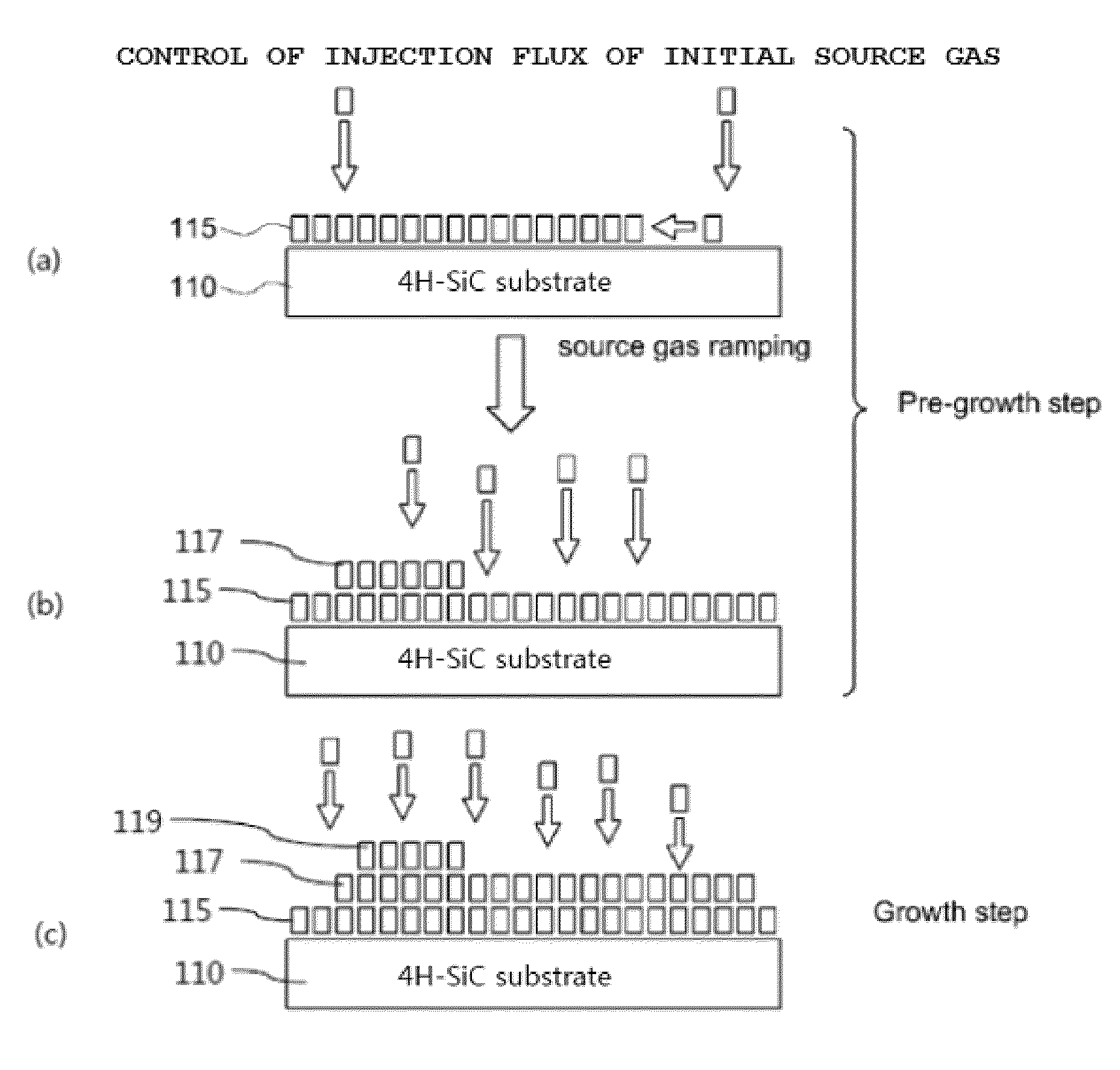
[0037]The surface defect density of the epitaxial wafer including an epitaxial layer grown on the substrate (or wafer) may be changed according to parameters such as flux of initial reactive gas, growth temperature, pressure, total flux, C / Si rat...


PUM


Abstract

Disclosed is an epitaxial wafer including a substrate, and an epitaxial structure disposed on the substrate, wherein the epitaxial structure includes a first epitaxial layer, a second epitaxial layer disposed on the first epitaxial layer, and a third epitaxial layer disposed between the first epitaxial layer and the second epitaxial layer, the third epitaxial layer having a first doping concentration around a first boundary adjacent to the first epitaxial layer and a second doping concentration different from the first doping concentration around a second boundary adjacent to the second epitaxial layer.

Description

CROSS REFERENCE TO RELATED APPLICATIONS[0001]This application claims the benefit under 35 U.S.C. §119 to Korean Application Nos. 10-2012-0122006, filed Oct. 31, 2012, and 10-2012-0122004, filed Oct. 31, 2012, which are hereby incorporated by reference in their entirety.FIELD OF THE INVENTION[0002]Embodiments relate to an epitaxial wafer, a method for fabricating the same and a semiconductor device including the same.BACKGROUND OF THE INVENTION[0003]Epitaxial growth generally includes a chemical vapor deposition process. In accordance with the epitaxial growth, a wafer is heated while a gas / liquid / solid silicon composite is transferred to a surface of a single crystal silicon wafer (or substrate) to be thermally decomposed or to have an effect on thermal decomposition. At this time, an epitaxial wafer is fabricated by laminating silicon onto a single crystal silicon wafer through continuous growth of a single crystal structure. In this case, defects such as lattice mismatch of aggreg...

Claims


Application Information

Patent Timeline
Patent Type & Authority Applications(United States)
IPC IPC(8): H01L21/02H01L29/165H01L29/16
CPCH01L21/02529H01L29/1608H01L29/165H01L21/02378H01L21/02447H01L21/02502H01L21/02576H01L21/02579H01L21/0262
Inventor KANG, SEOK MIN
Owner LG INNOTEK CO LTD
Why Eureka
Try Eureka