A kind of preparation method of n-type low-defect silicon carbide epitaxial wafer

A low-defect, silicon carbide technology, applied in semiconductor/solid-state device manufacturing, electrical components, circuits, etc., can solve the problems of reduced epitaxial layer quality, long consumption time, limited effect of ultra-thick silicon carbide epitaxial wafers, etc., and achieve cleaning cycle The effect of elongation, simple production method, and reduced growth cost

Active Publication Date: 2018-12-04
GLOBAL ENERGY INTERCONNECTION RES INST CO LTD +2
View PDF3 Cites 0 Cited by
  • Summary
  • Abstract
  • Description
  • Claims
  • Application Information

AI Technical Summary

Problems solved by technology

[0003] The traditional method is to reduce defects by adding a buffer layer between the substrate and the epitaxial layer, which has a certain effect on thin epitaxial wafers, but has limited effect on ultra-thick silicon carbide epitaxial wafers, due to the growth of ultra-thick silicon carbide epitaxial wafers. It takes a long time to process the epitaxial layer, and the environment in the growth chamber deteriorates with time, especially the deposits around and on the top, which will greatly reduce the quality of the epitaxial layer. Preparation method of ultra-thick silicon carbide epitaxial wafer

Method used


Image

  • A kind of preparation method of n-type low-defect silicon carbide epitaxial wafer
  • A kind of preparation method of n-type low-defect silicon carbide epitaxial wafer
  • A kind of preparation method of n-type low-defect silicon carbide epitaxial wafer

Examples


Embodiment 1

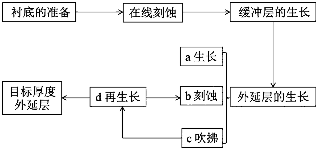
[0033] A method for preparing an N-type low-defect silicon carbide epitaxial wafer with a thickness of 15 μm, comprising the following steps:

[0034] 1) On-line etching of the substrate: prepare a substrate made of 4H-SiC, vacuumize, feed in hydrogen gas at a flow rate of 40L / min and HCl at a rate of 5L / min, the pressure in the reaction chamber is 40mbar, the temperature is 1680°C, and the temperature is maintained for 5 minute;

[0035] 2) Growth of the buffer layer: Stop feeding HCl, lower the temperature to 1650°C, and feed SiH with a flow rate of 6mL / min 4 and 3mL / min of C 3 h 8 , with the flow rate of 1500mL / min N 2 As a dopant, the growth pressure is 40mbar, and a buffer layer with a thickness of 0.4μm is grown;

[0036] 3) Growth of epitaxial layer

[0037] a Growth: 40L / min flow rate of hydrogen, 10mL / min SiH 4 and 5mL / min of C 3 h 8 Pass into the reaction chamber, keep the temperature at 1650°C, the pressure at 40mbar, and the N at a flow rate of 800mL / min 2...

Embodiment 2

[0042] A method for preparing an N-type low-defect silicon carbide epitaxial wafer with a thickness of 30 μm, comprising the following steps:

[0043] 1) On-line etching of the substrate: prepare a substrate made of 4H-SiC, vacuumize, feed in hydrogen gas at a flow rate of 40L / min and HCl at a rate of 5L / min, the pressure in the reaction chamber is 40mbar, the temperature is 1680°C, and the temperature is maintained for 5 minute;

[0044] 2) Growth of the buffer layer: Stop feeding HCl, lower the temperature to 1650°C, and feed SiH with a flow rate of 6mL / min 4 and 3mL / min of C 3 h 8 , with the flow rate of 1500mL / min N 2 As a dopant, the growth pressure is 40mbar, and a buffer layer with a thickness of 1 μm is grown;

[0045] 3) Growth of epitaxial layer

[0046] a Growth: 40L / min flow rate of hydrogen, 10mL / min SiH 4 and 5mL / min of C 3 h 8 Pass into the reaction chamber, keep the temperature at 1650°C, the pressure at 40mbar, and the N at a flow rate of 800mL / min 2 ...

Embodiment 3

[0054] A method for preparing an N-type low-defect silicon carbide epitaxial wafer with a thickness of 80 μm, comprising the following steps:

[0055] 1) On-line etching of the substrate: prepare a substrate made of 4H-SiC, vacuumize, feed in hydrogen gas at a flow rate of 40L / min and HCl at a rate of 5L / min, the pressure in the reaction chamber is 40mbar, the temperature is 1680°C, and the temperature is maintained for 5 minute;

[0056] 2) Growth of the buffer layer: Stop feeding HCl, lower the temperature to 1650°C, and feed SiH with a flow rate of 6mL / min 4 and 3mL / min of C 3 h 8 , with the flow rate of 1500mL / min N 2 As a dopant, the growth pressure is 40mbar, and a 1.5μm thick buffer layer is grown;

[0057] 3) Growth of epitaxial layer

[0058] a Growth: 40L / min flow rate of hydrogen, 10mL / min SiH 4 and 5mL / min of C 3 h 8 Pass into the reaction chamber, keep the temperature at 1650°C, the pressure at 40mbar, and the N at a flow rate of 800mL / min 2 As a dopant, ...


PUM

PropertyMeasurementUnit
thicknessaaaaaaaaaa
thicknessaaaaaaaaaa
thicknessaaaaaaaaaa

Abstract

The invention provides a preparation method of an N-type low-defect silicon carbide epitaxial wafer. The method comprises the steps of preparation of a substrate, online substrate etching, growth of a buffer layer and growth of an epitaxial layer, wherein growth of the epitaxial layer includes growth, etching, blowing and re-growth. The method can be used to effectively reduce the dislocation density of the base, reduce deposit in the cavity, reduce the defect density of the surface of the silicon carbide epitaxial wafer, improve the quality of a silicon carbide epitaxial material, and is wide in application range, low in processing cost and suitable for industrial production.

Description

technical field [0001] The invention relates to a method for preparing a semiconductor material, in particular to a method for preparing a silicon carbide epitaxial wafer. Background technique [0002] Silicon carbide (SiC) is the third-generation semiconductor material developed after the first-generation semiconductor materials silicon, germanium and the second-band semiconductor materials gallium arsenide and indium phosphide. The wide bandgap of silicon carbide materials is silicon and arsenide 2-3 times that of gallium, so that semiconductor devices can work at a relatively high temperature (above 500 ° C) and have the ability to emit blue light; the high breakdown electric field is an order of magnitude higher than that of silicon and gallium arsenide, which determines As a semiconductor device, SiC has the characteristics of high voltage and high power, high saturation electron drift velocity and low dielectric constant, and has high frequency and high speed working p...

Claims


Application Information

Patent Timeline
Patent Type & Authority Patents(China)
IPC IPC(8): H01L21/322H01L21/205H01L21/3065
CPCH01L21/02378H01L21/02656
Inventor 钮应喜杨霏
Owner GLOBAL ENERGY INTERCONNECTION RES INST CO LTD
Why Eureka
Try Eureka