Surface treatment method for molecular beam epitaxy InAs substrate
A molecular beam epitaxy and surface treatment technology, applied in chemical instruments and methods, polishing compositions containing abrasives, single crystal growth, etc., can solve the problems of difficult surface deoxidation, particle contamination, scratches, etc. , reduce pollution, avoid the effect of increasing
- Summary
- Abstract
- Description
- Claims
- Application Information
AI Technical Summary
Problems solved by technology
Method used
Image


Examples
Embodiment 1
[0059] Example 1 Surface Treatment of InAs Substrate for Molecular Beam Epitaxy
[0060] 1. Chemical mechanical polishing: use composite polishing pad, Gnad41 grinding and polishing machine for polishing, the polishing liquid is alkaline polishing liquid, the pressure is 310 g / cm 2 , the speed is 85 rpm, the polishing liquid is supplied by a roller pump non-circulating dripping (vacuum extrusion), and the flow rate is 300 mL / min;
[0061] Alkaline polishing liquid is composed of the following components by weight percentage (excluding organic acids): 10% colloidal silica, 11% oxidizing agent; 1% chelating agent and 78% deionized water; organic acid adjusts the pH value of the polishing liquid to 10 ;
[0062] The oxidant is composed of hydrogen peroxide, sodium hypochlorite and ammonium persulfate in a mass ratio of 1:1:0.5; the organic sodium salt is composed of sodium citrate, sodium tartrate and sodium benzenesulfonate in a mass ratio of 1:1:1 ;The organic acid is made up...
Embodiment 2
[0065] Example 2 Surface Treatment of InAs Substrate for Molecular Beam Epitaxy
[0066] 1. Chemical mechanical polishing: use composite polishing pad, Gnad41 grinding and polishing machine for polishing, the polishing liquid is alkaline polishing liquid, the pressure is 400 g / cm 2 , the speed is 95 rpm, and the polishing liquid is supplied by the non-circulating dripping (vacuum extrusion) method of the diaphragm pump, and the flow rate is 400 mL / min;
[0067] The alkaline polishing liquid is composed of the following components by weight percentage (excluding organic acids): 15% colloidal silica, 13% oxidizing agent; 3% chelating agent and 69% deionized water; the pH value of the polishing liquid adjusted by organic acid is 10 ;
[0068] The oxidant is composed of hydrogen peroxide, sodium hypochlorite and ammonium persulfate in a volume ratio of 1:1:0.5; the organic sodium salt is composed of sodium citrate, sodium tartrate and sodium benzenesulfonate in a mass ratio of 1:...
PUM
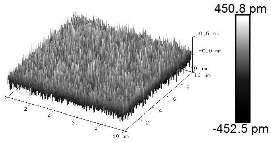
| Property | Measurement | Unit |
|---|---|---|
| Roughness | aaaaa | aaaaa |
Abstract
Description
Claims
Application Information