Method and system for improving critical dimension uniformity using shaped beam lithography

a technology of critical dimension and beam lithography, which is applied in the direction of photomechanical equipment, instruments, nuclear engineering, etc., to achieve the effect of reducing the maximum temperature of the surfa

Active Publication Date: 2014-05-08
D2S
View PDF1 Cites 15 Cited by
  • Summary
  • Abstract
  • Description
  • Claims
  • Application Information

AI Technical Summary

Benefits of technology

[0009]A method for forming a pattern on a surface using charged particle beam lithography is also disclosed, in which an ordered set of input shots is input, and in which a blanking period following a shot is lengthened to reduce the maximum temperature of the surface.

Problems solved by technology

An example of an end-use limitation is defining the geometry of a transistor in a way in which it cannot sufficiently operate at the required supply voltage.
The design rule limitations reflect, among other things, the smallest dimensions that can be reliably fabricated.

Method used


Image

  • Method and system for improving critical dimension uniformity using shaped beam lithography
  • Method and system for improving critical dimension uniformity using shaped beam lithography
  • Method and system for improving critical dimension uniformity using shaped beam lithography

Examples


Embodiment Construction

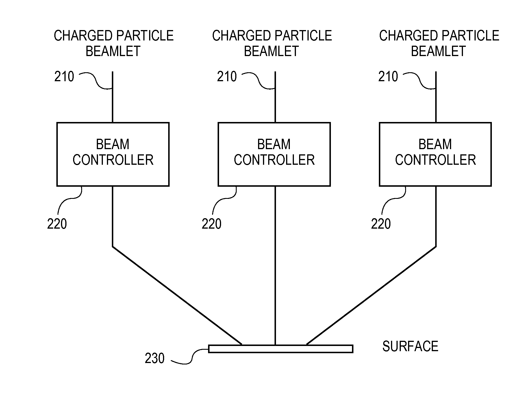
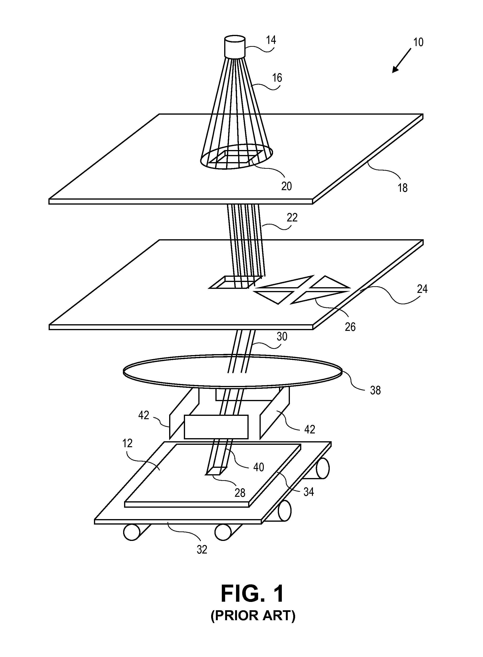
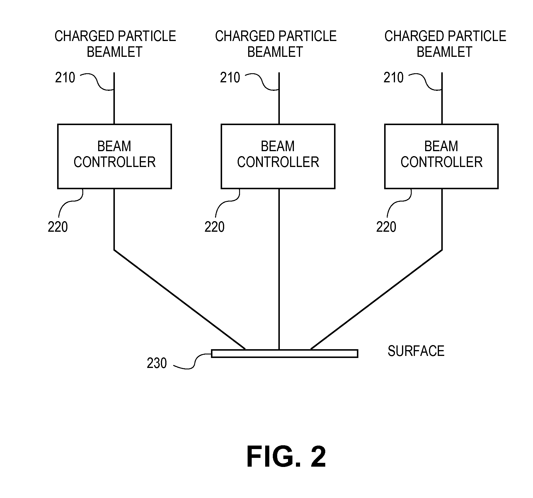
[0034]The present disclosure is related to lithography, and more particularly to the design and manufacture of a surface which may be a reticle, a wafer, or any other surface, using charged particle beam lithography.

[0035]As the size of shapes that are to be formed on a surface such as a reticle decreases in newer fabrication technologies, higher precision resists are being used to form these patterns. The sensitivity of these higher-precision resists is lower than for resists used for larger fabrication technologies. For example, common resists may have a sensitivity of 15 uC / cm2, but higher-precision resists more typically have a 25 uC / cm2 sensitivity. Even lower sensitivity resists, including some resists where sensitivity is >100 uC / cm2, are already used for some specific high-accuracy applications. The higher dosage required by the lower-sensitivity resists increases reticle write times. To help reduce this increase in write time caused by the lower-sensitivity resists, newer c...


PUM

PropertyMeasurementUnit
wavelengthaaaaaaaaaa
current densitiesaaaaaaaaaa
write timeaaaaaaaaaa

Abstract

A method for forming a pattern on a surface using charged particle beam lithography is disclosed, where the shots in an ordered set of input shots are modified within a subfield to reduce either a thermal variation or a maximum temperature of the surface during exposure by the charged particle beam writer. A method for fracturing or mask data processing is also disclosed, where an ordered set of shots is generated which will expose at least one subfield of a surface using a shaped beam charged particle beam writer, and where a temperature or a thermal variation generated on the surface during the exposure of one subfield is calculated. Additionally, a method for forming a pattern on a surface with an ordered set of shots using charged particle beam lithography is disclosed, in which a blanking period following a shot is lengthened to reduce the maximum temperature of the surface.

Description

[0001]This application claims priority to U.S. Provisional Patent Application Ser. No. 61 / 722,042 filed on Nov. 2, 2012 and entitled “Method and System For Improving Critical Dimension Uniformity Using Shaped Beam Lithography”, which is hereby incorporated by reference for all purposes.BACKGROUND OF THE DISCLOSURE[0002]In the production or manufacturing of semiconductor devices, such as integrated circuits, optical lithography may be used to fabricate the semiconductor devices. Optical lithography is a printing process in which a lithographic mask or photomask manufactured from a reticle is used to transfer patterns to a substrate such as a semiconductor or silicon wafer to create the integrated circuit (I.C.). Other substrates could include flat panel displays, holographic masks or even other reticles. While conventional optical lithography uses a light source having a wavelength of 193 nm, extreme ultraviolet (EUV) or X-ray lithography are also considered types of optical lithogra...

Claims


Application Information

Patent Timeline
Patent Type & Authority Applications(United States)
IPC IPC(8): G03F7/20
CPCG03F7/70275G03F7/20H01J37/3174H01J37/3026H01J2237/31764H01J2237/31776B82Y10/00B82Y40/00G03F7/70533G03F7/2051G03F7/2065G03F7/2059
Inventor FUJIMURA, AKIRAPEARMAN, RYANAADAMOV, ANATOLY
Owner D2S
Why Eureka
Try Eureka