

Sic epitaxial wafer and method for producing same, and device for producing sic epitaxial wafer
a technology of epitaxial wafers and manufacturing methods, which is applied in the direction of crystal growth process, polycrystalline material growth, chemically reactive gases, etc., can solve the problems of deterioration in the quality of the epitaxial layer, material pieces falling, and deterioration in the shielding plate hardly progresses
- Summary
- Abstract
- Description
- Claims
- Application Information
AI Technical Summary
Benefits of technology
Problems solved by technology
Method used
Image

Examples
first embodiment
[SiC Epitaxial Wafer Manufacturing Apparatus (First Embodiment)]
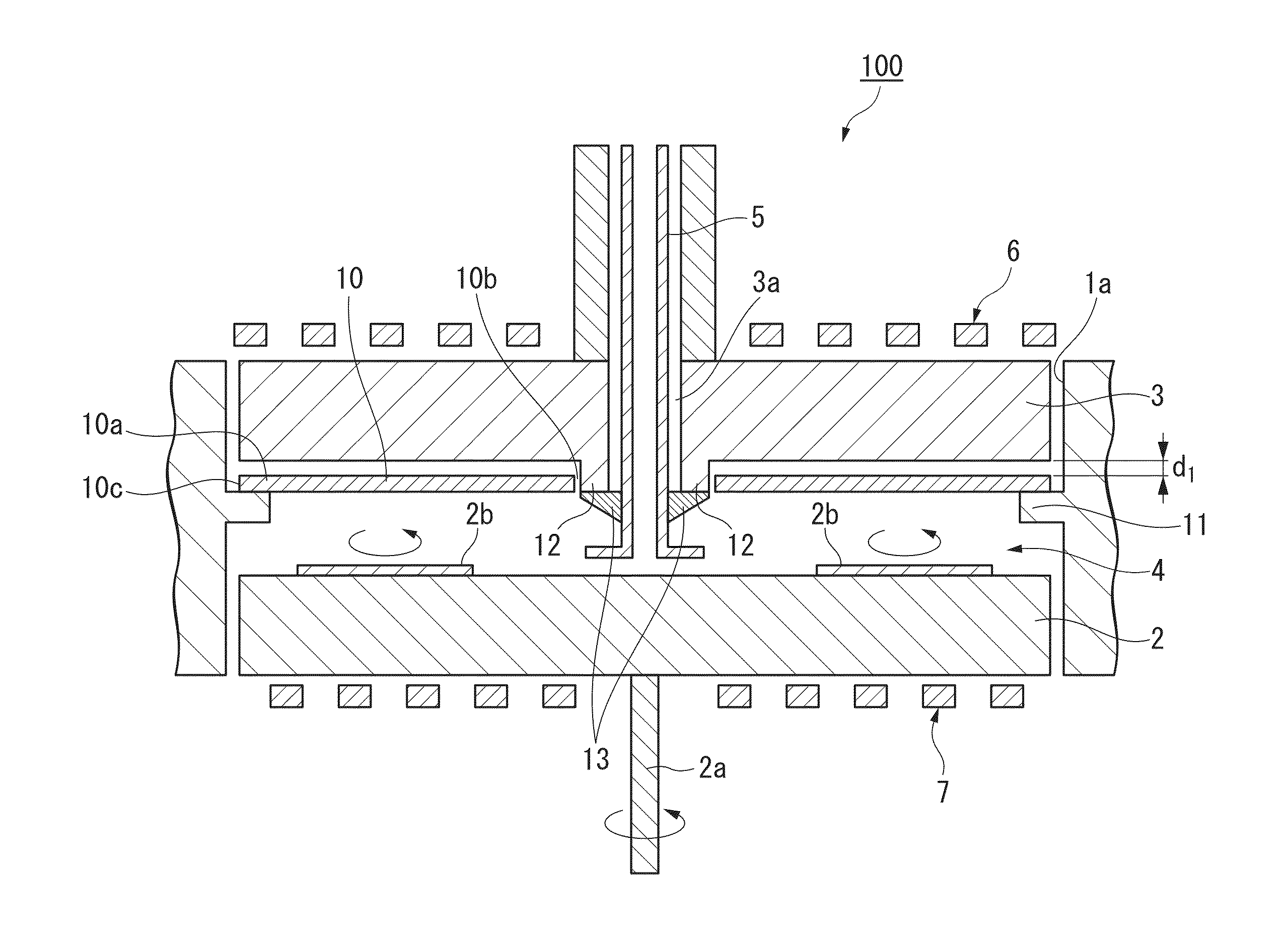
[0098]FIG. 5 is a schematic sectional view illustrating a part of an epitaxial wafer manufacturing apparatus to which the present invention is applied. FIG. 6 is a perspective view illustrating a lower side of the epitaxial wafer manufacturing apparatus taken along the line A-A′ of FIG. 5. FIG. 7 is a schematic expanded view of the periphery of a shielding plate shown in FIG. 5.
[0099]An epitaxial wafer manufacturing apparatus 100 according to an embodiment herein is, for example, a CVD apparatus 100 illustrated in FIG. 5. Specifically, the epitaxial wafer manufacturing apparatus 100 includes a plurality of placement units 2b on which a wafer is placed, a susceptor 2 for which the plurality of placement units 2b are arranged in tandem in a circumferential direction, a sealing (top plate) 3 disposed to face the upper surface of the susceptor 2 so that a reaction space 4 is formed in a space between the susceptor 2 and the...
second embodiment
[SiC Epitaxial Wafer Manufacturing Apparatus (Second Embodiment)]
[0135]An epitaxial wafer manufacturing apparatus according to an embodiment herein includes a susceptor that includes a wafer placement unit on which a wafer is placed and a sealing (top plate) that is disposed to face the upper surface of the susceptor so that a reaction space is formed between the sealing and the susceptor. The sealing is formed of silicon carbide or the surface of the sealing facing the susceptor is covered with a silicon carbide film or a pyrolytic carbon film, and an epitaxial layer is formed on a surface of the wafer while a raw material gas is supplied into a chamber. The epitaxial wafer manufacturing apparatus is different from the epitaxial wafer manufacturing apparatus according to the first embodiment in that a shielding plate is not provided.
[0136]In the epitaxial wafer manufacturing apparatus, since material pieces falling on the wafer from the sealing are reduced, it is possible to manufa...
examples
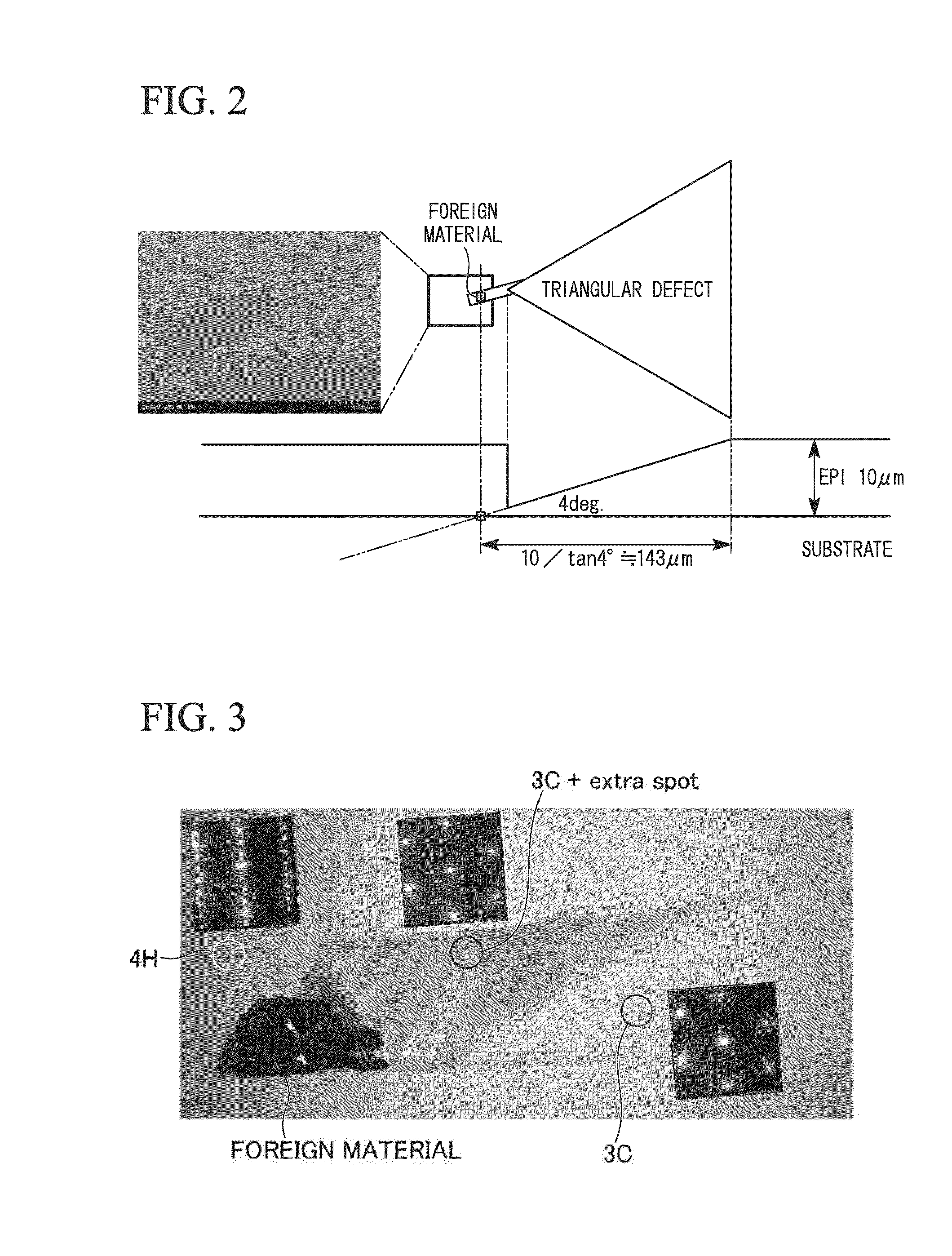
[0172]Hereinafter, the advantageous effects of the present invention will be described specifically according to examples. The present invention is not limited to these examples.
PUM
| Property | Measurement | Unit |
|---|---|---|
| thickness | aaaaa | aaaaa |
| horizontal distance | aaaaa | aaaaa |
| horizontal distance | aaaaa | aaaaa |
Abstract
Description
Claims
Application Information