Patterned substrate and electro-optical semiconductor element

a semiconductor element and electro-optical technology, applied in the field of electro-optical semiconductor elements, can solve the problems of not meeting higher requirements, limiting the improvement of the electro-optical efficiency of the optical components, and limited electro-optical efficiency of the existing optical components, so as to increase increase the light scattering, refraction and diffraction, and enhance the electro-optical efficiency of the electro-optical semiconductor elements

Inactive Publication Date: 2014-06-12
LUCEMITEK
View PDF2 Cites 0 Cited by
  • Summary
  • Abstract
  • Description
  • Claims
  • Application Information

AI Technical Summary

Benefits of technology

[0026]As mentioned above, the solid patterns of the patterned substrate are irregularly arranged. For example, at least partial pitches between the solid patterns are different, or at least partial spaces between the solid patterns are different. Accordingly, the contact situations of the incident light and the solid patterns are increased, thereby enhancing the electro-optical efficiency of the electro-optical semiconductor element. For example, the incident light may enter the solid patterns or be reflected by the surface of the solid patterns.
[0027]In additio...

Problems solved by technology

Accordingly, the uniform included angle and smooth surface can restrict the improvement of the electro-optical efficiency of the optical c...

Method used


Image

  • Patterned substrate and electro-optical semiconductor element
  • Patterned substrate and electro-optical semiconductor element
  • Patterned substrate and electro-optical semiconductor element

Examples


Embodiment Construction

[0037]The present invention will be apparent from the following detailed description, which proceeds with reference to the accompanying drawings, wherein the same references relate to the same elements.

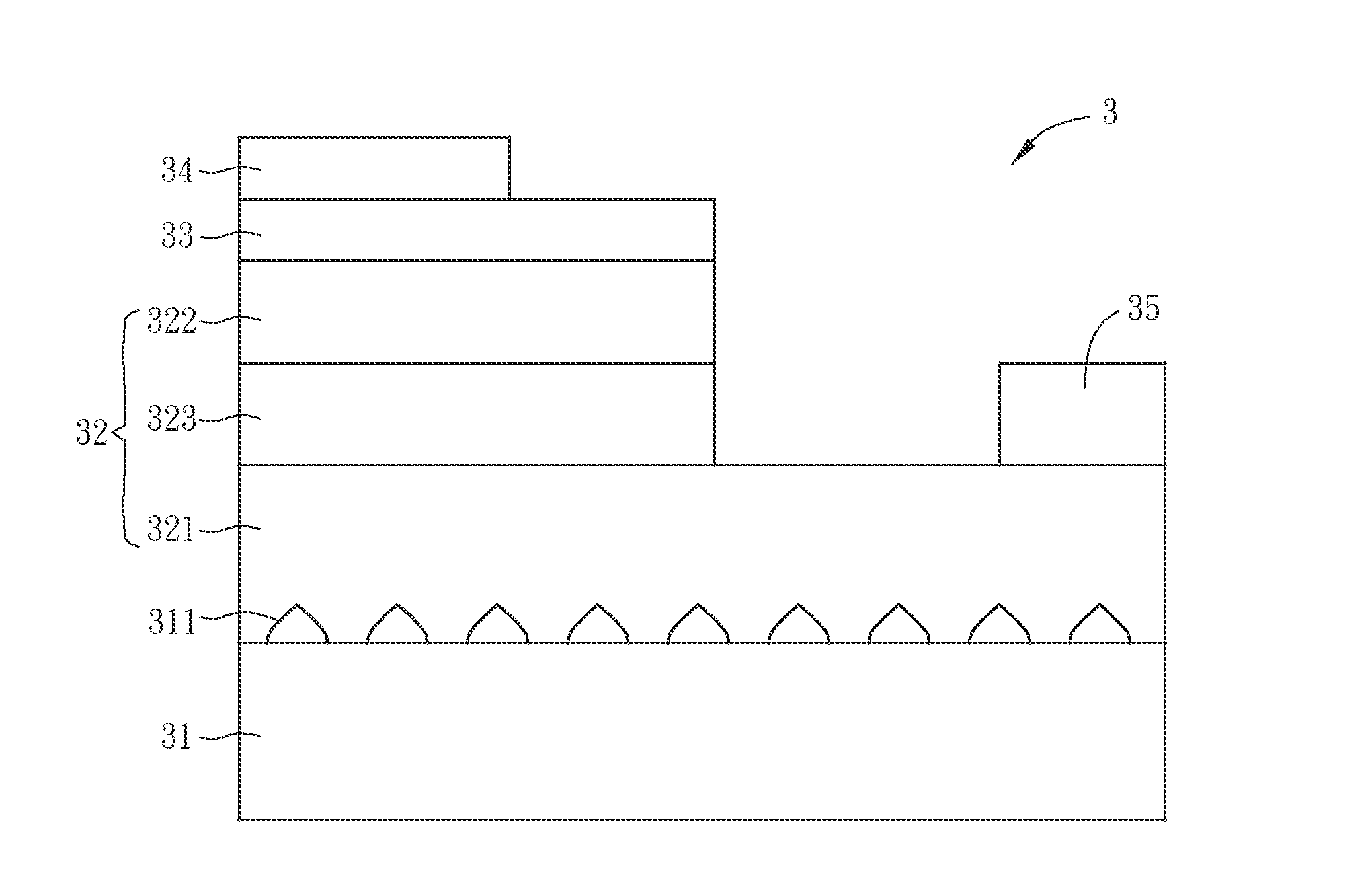
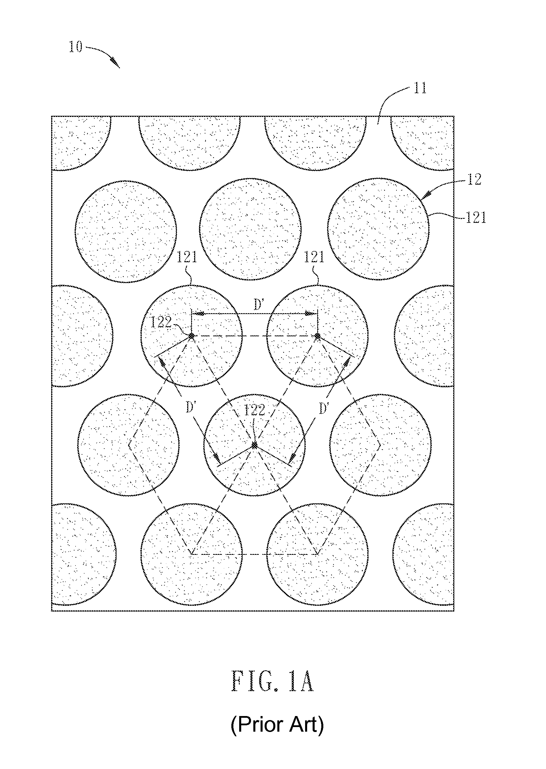
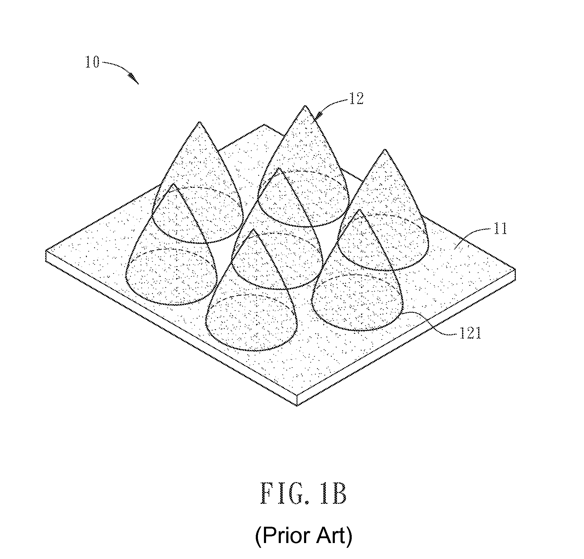
[0038]FIG. 2A is a schematic top view of a part of a patterned substrate according to a preferred embodiment of the invention, and FIG. 2B is a schematic diagram of the solid patterns in FIG. 2A. As shown in FIGS. 2A and 2B, the patterned substrate 20 includes a substrate body 21 and a plurality of solid patterns 22 disposed on the substrate body 21. The substrate body 21 can be a sapphire substrate, a silicon substrate, a silicon carbide substrate, a spinel substrate, or a polymer substrate for example. To be noted, the sapphire substrate further can be a c-plane (0001) sapphire substrate. Otherwise, the substrate body 21 can be a silica substrate, a silicon nitride substrate, an aluminum nitride substrate, a diamond substrate or a diamond-like carbon substrate.

[0039]FIG. 2A is a top...


PUM


Abstract

A patterned substrate includes a substrate body and a plurality of solid patterns. The solid patterns are set on the substrate body, and at least partial pitches between the solid patterns are different.

Description

CROSS REFERENCE TO RELATED APPLICATIONS[0001]This Non-provisional application claims priority under 35 U.S.C. §119(a) on Patent Application No(s). 101146962 filed in Taiwan, Republic of China on Dec. 12, 2012, the entire contents of which are hereby incorporated by reference.BACKGROUND OF THE INVENTION[0002]1. Field of Invention[0003]The invention relates to an electro-optical semiconductor element and, in particular, to an electro-optical semiconductor element with enhanced electro-optical efficiency.[0004]2. Related Art[0005]The electro-optical semiconductor element has been widely applied to various fields, such as illumination, vehicles, display apparatuses, communication industry and computers.[0006]A conventional electro-optical semiconductor element includes a substrate body and a plurality of solid patterns disposed on a surface of the substrate body. The solid patterns are arranged into a row regularly, so the substrate is regarded as a patterned structural substrate (PSS) ...

Claims


Application Information

Patent Timeline
IPC IPC(8): H01L31/02H01L33/48
CPCH01L33/007H01L33/20H01L31/056Y02E10/52Y10T428/24355
Inventor CHIU, CHENG-YULEE, CHUN-YICHEN, CHUN-HUNGCHEN, CHIH-ANWANG, WEI-LUN
Owner LUCEMITEK
Why Eureka
Try Eureka