Semiconductor structure and process thereof

Active Publication Date: 2014-06-12
UNITED MICROELECTRONICS CORP
View PDF6 Cites 13 Cited by
  • Summary
  • Abstract
  • Description
  • Claims
  • Application Information

AI Technical Summary

Benefits of technology

[0009]According to the above, the present invention provides a semiconductor structure and a process thereof, which performs two in-situ annealing processes on a dielectric layer, and the two annealing processes have different imported gases and different annealing temperatures. In this way, the dielectric layer and a substrate can be repaired effectively by performing the two annealing processes having different imported gases and different annealing temperatures, and a circuit leakage density (Jg) is therefore reduced. Moreover, only one single pre-heating or heating step is performed as the two annealing processes having different imported gases and different annealing temperatures are performed, thereby shortening the processing time of the two annealing processes. Besides, the d

Problems solved by technology

Moreover, only one single pre-heating or heating step is performed as the two annealing processes having different imported ga

Method used


Image

  • Semiconductor structure and process thereof
  • Semiconductor structure and process thereof
  • Semiconductor structure and process thereof

Examples


Example

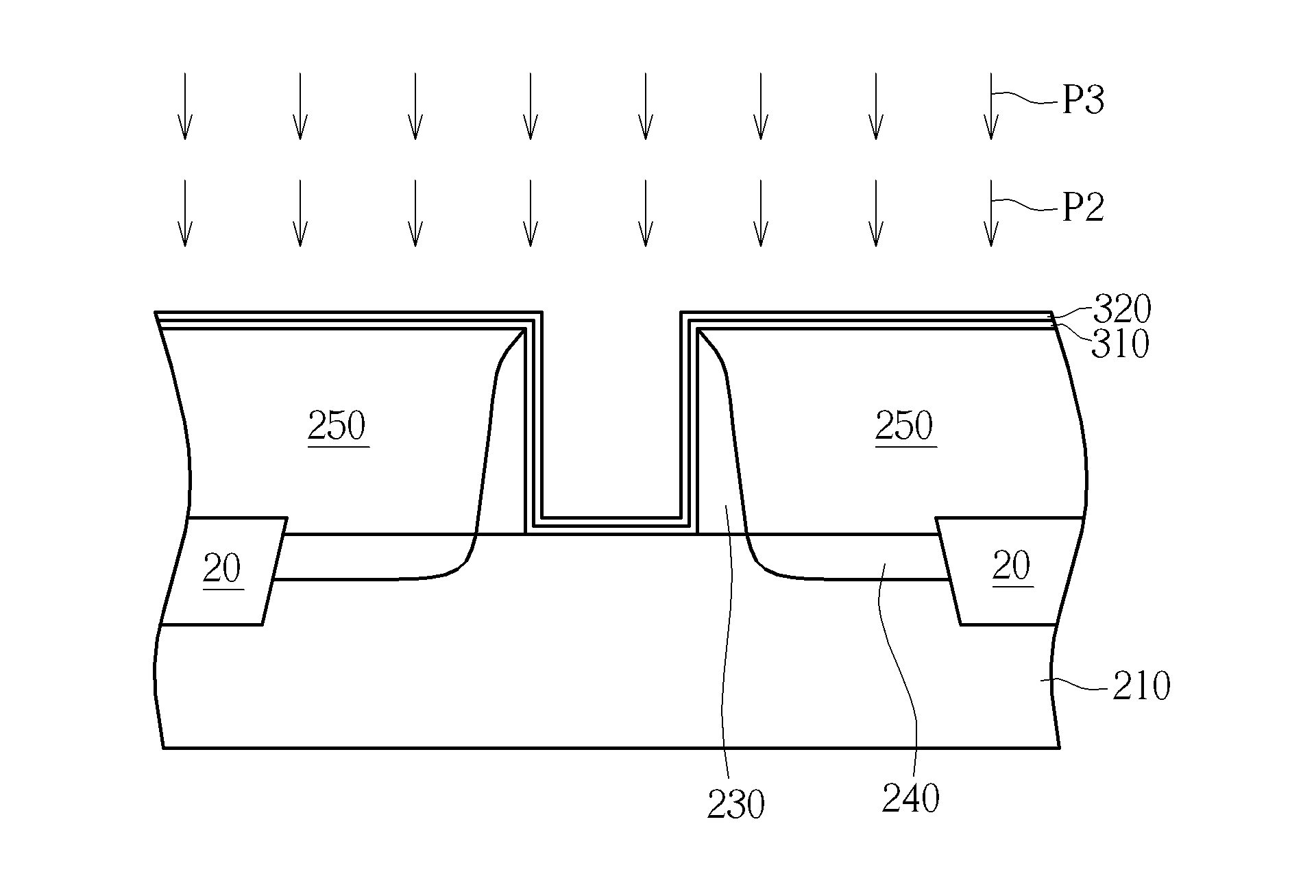
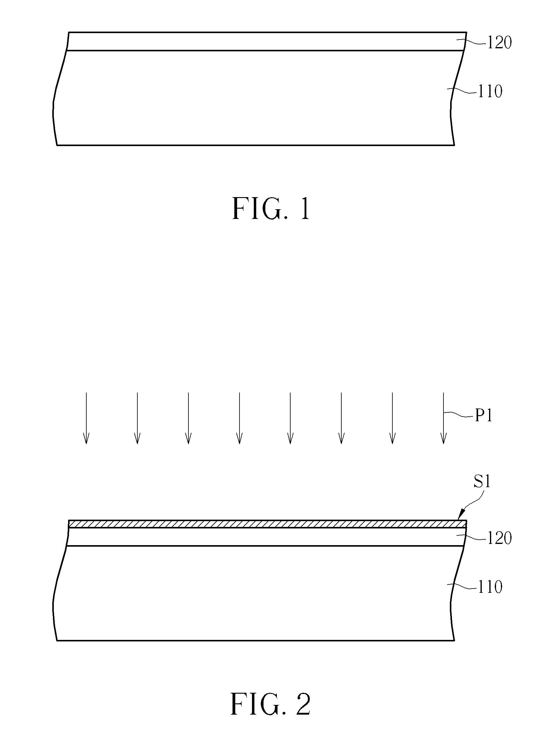
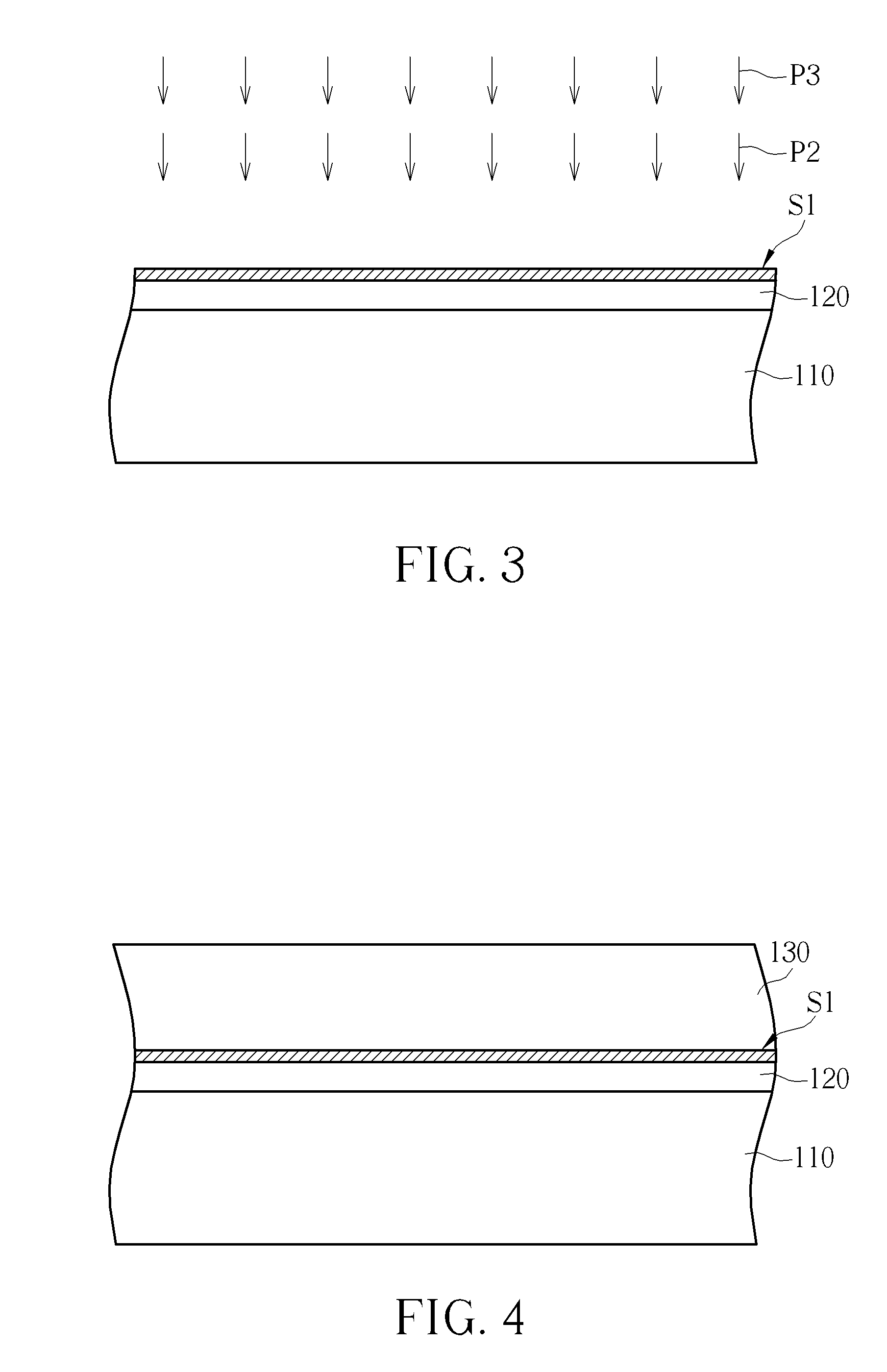
[0016]FIGS. 1-4 schematically depict cross-sectional views of a semiconductor process according to an embodiment of the present invention. A shown in FIG. 1, a substrate 110 is provided. The substrate 110 may be a semiconductor substrate such as a silicon substrate, a silicon containing substrate, a III-V group-on-silicon (such as GaN-on-silicon) substrate, a graphene-on-silicon substrate or a silicon-on-insulator (SOI) substrate. A dielectric layer 120 is formed on the substrate 110. The dielectric layer 120 maybe a silicon oxide layer, a silicon oxynitride layer or a hafnium oxide layer or a combination thereof, but it is not limited thereto. The semiconductor process of the present invention is suited for being applied in gate processes such as in a polysilicon gate process, a gate last process or a gate first process, wherein the gate last process includes a gate last process for buffer layer first and High-K first process, a gate last process for buffer layer first and High-K l...


PUM


Abstract

A semiconductor structure includes a dielectric layer located on a substrate, wherein the dielectric layer includes nitrogen atoms, and the concentration of the nitrogen atoms in the dielectric layer is lower than 5% at a location wherein the distance between this location in the dielectric layer to the substrate is less than 20% of the thickness of the dielectric layer. Moreover, the present invention provides a semiconductor process including the following steps: a dielectric layer is formed on a substrate. Two annealing processes are performed in-situly on the dielectric layer, wherein the two annealing processes have different imported gases and different annealing temperatures.

Description

BACKGROUND OF THE INVENTION[0001]1. Field of the Invention[0002]The present invention relates generally to a semiconductor structure and a process thereof, and more specifically to a semiconductor structure and a process thereof that performs two in-situ annealing processes on a dielectric layer.[0003]2. Description of the Prior Art[0004]Poly-silicon is conventionally used as a gate electrode in semiconductor devices, such as the metal-oxide-semiconductors (MOS). With the trend towards scaling down the size of semiconductor devices, however, conventional poly-silicon gates face problems such as inferior performances due to boron penetration and unavoidable depletion effect. This increases the equivalent thickness of the gate dielectric layer, reduces the gate capacitance, and worsens a driving force of the devices. Therefore, work function metals are used to replace the conventional poly-silicon gate to be the control electrode, and to form metal gates.[0005]Dielectric layers are ne...

Claims


Application Information

Patent Timeline
IPC IPC(8): H01L21/02H01L21/441H01L29/06
CPCH01L21/02318H01L29/0603H01L21/441H01L21/02164H01L21/02332H01L21/02337H01L21/0234H01L21/3105H01L21/31155H01L21/28202H01L29/4966H01L29/51H01L29/513H01L29/66545H01L29/78H01L21/28185H01L29/517
Inventor LIN, CHIEN-LIANGWANG, YU-RENYEN, YING-WEI
Owner UNITED MICROELECTRONICS CORP
Why Eureka
Try Eureka