Circuit configuration and manufacturing processes for vertical transient voltage suppressor (TVS) and EMI filter

a technology of transient voltage suppressor and manufacturing process, which is applied in the direction of semiconductor devices, semiconductor/solid-state device details, diodes, etc., can solve the problems of large area to reduce resistance, uncontrollable bight voltage may accidentally strike the circuit, and damage to the circuit, etc., and achieve the effect of small silicon die footprin

Active Publication Date: 2014-06-19
ALPHA & OMEGA SEMICON INC
View PDF3 Cites 31 Cited by
  • Summary
  • Abstract
  • Description
  • Claims
  • Application Information

AI Technical Summary

Benefits of technology

[0009]It is therefore an aspect of the present invention to provide an improved vertical TVS and EMI filter circuit by applying DMOS technology implementing the mainstream DMOS processes to produce low-cost TVS and EMI filter circuits that has small silicon die footprint such that the above discussed limitations and difficulties can be overcome.

Problems solved by technology

However, in situations such as electrostatic discharge (ESD), electrical fast transients and lightning, an unexpected and an uncontrollable bight voltage may accidentally strike onto the circuit.
Since the Zener diode has higher resistance per unit area compared with BJT or SCR and BJT this is actually a disadvantage at higher currents because the steering diodes also have to be rugged in reverse conduction.
The problem with the Vcc-Gnd clamp diodes is that typically these diodes are very resistive in reverse blocking mode and require large area to reduce resistance.
This is not desirable as high BV not only causes the break down of steering diodes as described above but also causes damage to the circuit the TVS device intends to protect.
The requirement to have large diode size thus limits further miniaturization of a device when such TVS circuit is implemented.
Such vertical diode and EMI filter configurations as shown in FIGS. 1B-1 to 1C-2 suffer the disadvantage that there is great junction capacitance and has a poor clamping performance due to the high diode series resistance caused by the high resistivity of substrate.

Method used


Image

  • Circuit configuration and manufacturing processes for vertical transient voltage suppressor (TVS) and EMI filter
  • Circuit configuration and manufacturing processes for vertical transient voltage suppressor (TVS) and EMI filter
  • Circuit configuration and manufacturing processes for vertical transient voltage suppressor (TVS) and EMI filter

Examples


Embodiment Construction

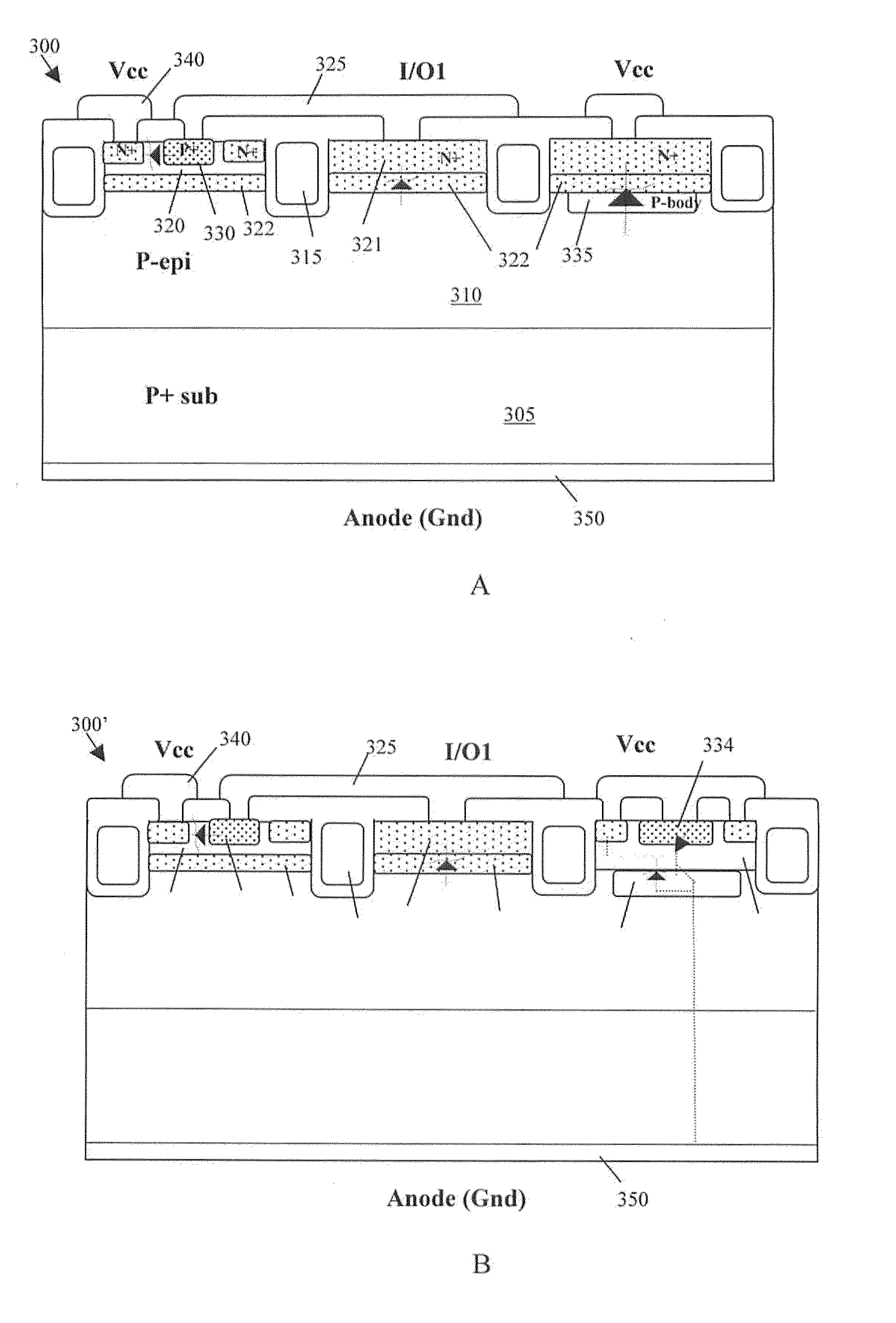
[0031]Refer to FIGS. 2A and 2B for a side cross sectional view and a circuit diagram of a vertical transient voltage suppressor (VTVS) 100 fabricated by using the standard DMOS process. The VTVS 100 is formed on a heavily doped semiconductor substrate 105 that includes a front side functioning as an anode terminal 110 and to backside functioning as a cathode terminal 120 for the vertical TVS that includes an inherent diode and NPN transistor. As the product is fabricated by applying standard trench DMOS process, the cross section in FIG. 2A shows a trench NMOS structure with source regions 125 formed over a body region 130 on top of a N epitaxialtaxial layer 115 over the 105 N+ substrate functioning as a drain. The insulated trench gates 135 interconnected with a gate runner 135-GR at the edge area through other trench gates in a third dimension. The difference of this VTVS device from a regular trench DMOS is that the gate runner 135-GR is shorted to the drain 105 by a gate metal 1...


PUM


Abstract

A vertical TVS (VTVS) circuit includes a semiconductor substrate for supporting the VTVS device thereon having a heavily doped layer extending to the bottom of substrate. Deep trenches are provided for isolation between multi-channel VTVS. Trench gates are also provided for increasing the capacitance of VTVS with integrated EMI filter.

Description

[0001]This Patent Application is a Divisional Application of a co-pending application Ser. No. 12 / 806,659 filed on Aug. 8, 2010 by the Applicants of this Application and application Ser. No. 12 / 806,659 is a Divisional Application of application Ser. No. 11 / 600,696 filed on Nov. 16, 2006 now issued as U.S. Pat. No. 7,781,826 on Aug. 24, 2010. The Disclosures made in the Patent application Ser. Nos. 11 / 600,696 and 12 / 806,659 are hereby incorporated by reference.BACKGROUND OF THE INVENTION[0002]1. Field of the Invention[0003]The invention relates generally to a circuit configuration and method of manufacture of a transient voltage suppressor (TVS). More particularly, this invention relates to an improved circuit configuration and method of manufacture of a vertical transient voltage suppressor (VTVS) with EMI filter.[0004]2. Description of the Relevant Art[0005]The transient voltage suppressors (TVS) are commonly applied for protecting integrated circuits from damages due to the inadve...

Claims


Application Information

Patent Timeline
Patent Type & Authority Applications(United States)
IPC IPC(8): H01L27/02H01L23/60H01L21/02H01L29/73
CPCH01L29/861H01L2924/0002H01L27/0255H01L29/407H01L29/0649H01L27/0727H01L2924/00H01L27/0248H01L21/02365H01L29/7304H01L23/60H01L29/7322
Inventor MALLIKARJUNASWAMY, SHEKARBOBDE, MADHUR
Owner ALPHA & OMEGA SEMICON INC
Why Eureka
Try Eureka