High density trench-based power mosfets with self-aligned active contacts and method for making such devices

a technology of active contacts and trenches, which is applied in the field of high density trenches-based power mosfets, can solve the problems of reducing the possibility of the device turning, increasing the rsub>dsa/sub>, and reducing the breakdown voltag

Active Publication Date: 2014-06-26
ALPHA & OMEGA SEMICON INC
View PDF13 Cites 21 Cited by
  • Summary
  • Abstract
  • Description
  • Claims
  • Application Information

AI Technical Summary

Problems solved by technology

Finally, minimizing the ratio of Qgd / Qgs reduces the possibility of the device turning on due to a large dV / dt when the device is being switched off.
However, the basic trench based MOSFET does not have any charge balancing in the body regions, and therefore causes an increase in the RdsA.
Also, the relatively thin gate oxide generates a high electric field under the trench, which leads to a lower breakdown voltage.
Further, as cell pitch continues to decrease, the trench based MOSFET may become a less desirable choice because of the difficulty in reducing the thickness of the gate oxide further.
Finally, complex processing is required in order to produce two electrically separated polysilicon electrodes within the same trench.
The complexity of the fabrication is further accentuated when the pitch of the device is scaled downwards to the deep sub-micron level.
However, the device shown in FIG. 4C is not easily downwards scalable because it is highly susceptible to body contact misalignment errors.
Also, if the contact mask is aligned too far away from the gate, then the turn on of the bipolar junction transistor (BJT) becomes an issue.

Method used


Image

  • High density trench-based power mosfets with self-aligned active contacts and method for making such devices
  • High density trench-based power mosfets with self-aligned active contacts and method for making such devices
  • High density trench-based power mosfets with self-aligned active contacts and method for making such devices

Examples


Embodiment Construction

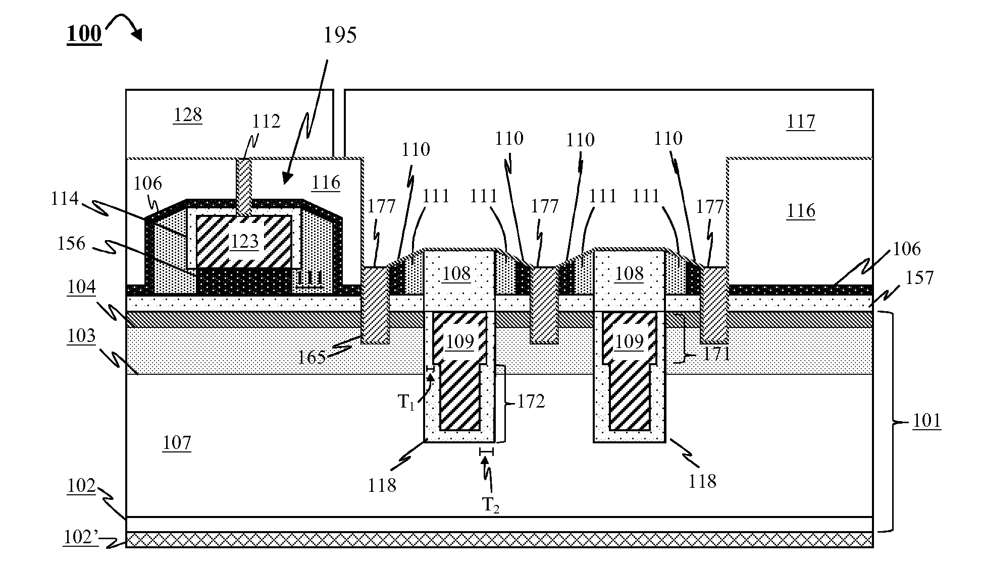
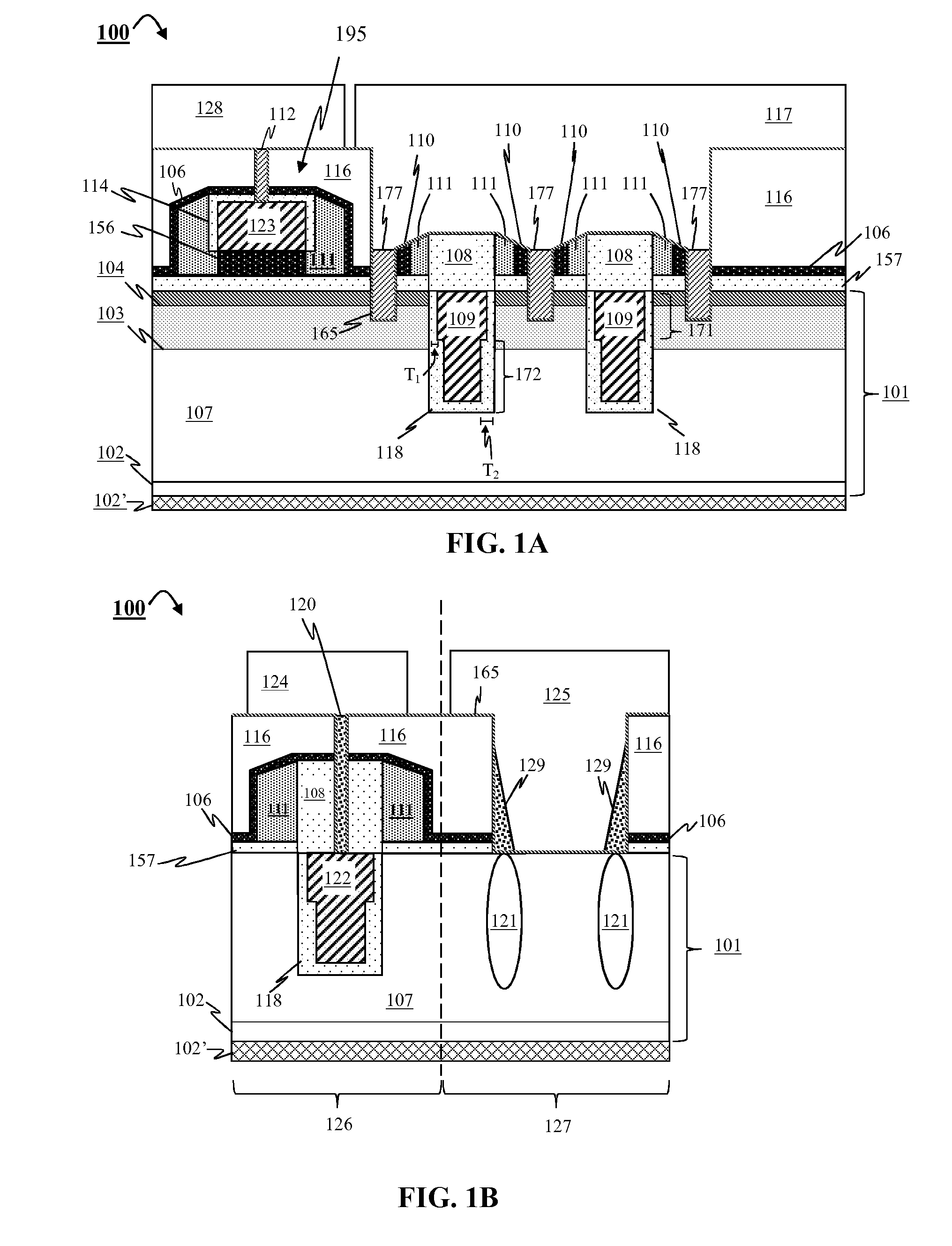
[0017]Although the following detailed description contains many specific details for the purposes of illustration, anyone of ordinary skill in the art will appreciate that many variations and alterations to the following details are within the scope of the invention. Accordingly, the exemplary embodiments of the invention described below are set forth without any loss of generality to, and without imposing limitations upon, the claimed invention. In the following discussion, an N-type device is described for purposes of illustration. P-type devices may be fabricated using a similar process but with opposite conductivity types.

[0018]According to aspects of the present disclosure high density trench-based power MOSFET may be fabricated with self-aligned source and body contacts. The source / body contacts are self-aligned with a first insulative spacer and a second insulative spacer. By way of example, the first spacer may be resistant to an etching process that will selectively remove ...


PUM


Abstract

Aspects of the present disclosure describe a high density trench-based power MOSFET with self-aligned source contacts. The source contacts are self-aligned with a first insulative spacer and a second insulative spacer, wherein the first spacer is resistant to an etching process that will selectively remove the material the second spacer is made from. Additionally, the active devices may have a two-step gate oxide, wherein a lower portion of the gate oxide has a thickness T2 that is larger than the thickness T1 of an upper portion of the gate oxide. It is emphasized that this abstract is provided to comply with rules requiring an abstract that will allow a searcher or other reader to quickly ascertain the subject matter of the technical disclosure. It is submitted with the understanding that it will not be used to interpret or limit the scope or meaning of the claims.

Description

CROSS-REFERENCE TO RELATED APPLICATIONS[0001]This application is related to commonly-assigned, co-pending application Ser. No. 13 / ______, (Attorney Docket Number ANO-058 / US), filed the same day as the present application and entitled “DEVICE STRUCTURE AND METHODS OF MAKING HIGH DENSITY MOSFETS FOR LOAD SWITCH AND DC-DC APPLICATIONS” to Yilmaz, Bobde, Chang, Lee, Calafut, Kim, Lui, and Chen, the entire disclosures of which are incorporated herein by reference.[0002]This application is related to commonly-assigned, co-pending application Ser. No. 13 / ______, (Attorney Docket Number ANO-059 / US), filed the same day as the present application and entitled “HIGH FREQUENCY SWITCHING MOSFETS WITH A LOW OUTPUT CAPACITANCE USING A DEPLETABLE P-SHIELD” to Bobde, Yilmaz, Lui, and Ng, the entire disclosures of which are incorporated herein by reference.FIELD OF THE INVENTION[0003]This invention generally relates to metal oxide silicon field effect transistors (MOSFETs) and more particularly to hi...

Claims


Application Information

Patent Timeline
Patent Type & Authority Applications(United States)
IPC IPC(8): H01L21/8234H01L21/28H01L29/78H01L29/423H01L21/033H01L29/66
CPCH01L21/3081H01L21/823456H01L21/823462H01L21/823468H01L29/42376H01L2924/0002H01L29/66553H01L29/6656H01L29/7813H01L29/6653H01L2924/00H01L27/0248H01L29/41766H01L21/28114H01L27/0251H01L23/66H01L27/0292H01L29/0619H01L29/1095H01L29/42364H01L29/66719H01L29/66734H01L29/7803H01L29/7811
Inventor LEE, YEEHENGCHANG, HONGKIM, JONGOHLIU, SIKYILMAZ, HAMZABOBDE, MADHURCALAFUT, DANIELCHEN, JOHN
Owner ALPHA & OMEGA SEMICON INC
Why Eureka
Try Eureka