Multijunction solar cell with low band gap absorbing layer in the middle cell

a solar cell and middle cell technology, applied in the field of solar cells and the fabrication of solar cells, can solve the problems of reducing the overall current flow through the circuit, affecting the efficiency of solar cells, so as to achieve the effect of increasing the photoconversion efficiency

Inactive Publication Date: 2014-07-03
SOLAERO TECH CORP
View PDF3 Cites 42 Cited by
  • Summary
  • Abstract
  • Description
  • Claims
  • Application Information

AI Technical Summary

Benefits of technology

[0023]It is an object of the present invention to provide increased photoconversion efficiency in a multijunction solar cell.

Problems solved by technology

Compared to silicon, III-V compound semiconductor multijunction devices have greater energy conversion efficiencies and generally more radiation resistance, although they tend to be more complex to manufacture.
Mismatching of the lattice constant between adjacent semiconductor layers in the solar cells results in defects or dislocations in the crystal, which in turn causes degradation of photovoltaic efficiency by undesirable phenomena known as open-circuit voltage, short circuit current, and fill factor.
In a series electrical circuit, the overall current flows though the circuit is limited to the smallest current capability of any one of the individual cells in the circuit.
However, these prior art solar cell layers have often been lattice mismatched, which may lead to photovoltaic quality degradation and reduced efficiency, even for slight mismatching, such as less than one percent.
Further, even when lattice-matching is achieved, these prior art solar cells often fail to obtain desired photovoltage outputs.
This low efficiency is caused, at least in part, by the difficulty of lattice-matching each semiconductor cell to commonly used and preferred materials for the substrate, such as germanium (Ge) or gallium-arsenide (GaAs) substrates.
However, the limited selection of known semiconductor materials, and corresponding band gaps, that have the same lattice constant as the above preferred substrate materials has continued to make it a challenge to design and fabricate multijunction solar cells with high conversion efficiency and reasonable manufacturing yields.
However, one problem associated with the conventional multijunction solar cell structure is the relatively low performance relating to the homojunction middle solar cells in the multijunction solar cell structures.
The performance of a homojunction solar cell is typically limited by the material quality of the emitter, which is low in homojunction devices.
Low material quality usually includes such factors as poor surface passivation, lattice mismatch between layers and / or narrow band gaps of the selected material.
Increasing device efficiency of multijunction solar cell structures through band-gap engineering and lattice matching alone, however, has proven increasingly challenging.

Method used


Image

  • Multijunction solar cell with low band gap absorbing layer in the middle cell
  • Multijunction solar cell with low band gap absorbing layer in the middle cell
  • Multijunction solar cell with low band gap absorbing layer in the middle cell

Examples


first embodiment

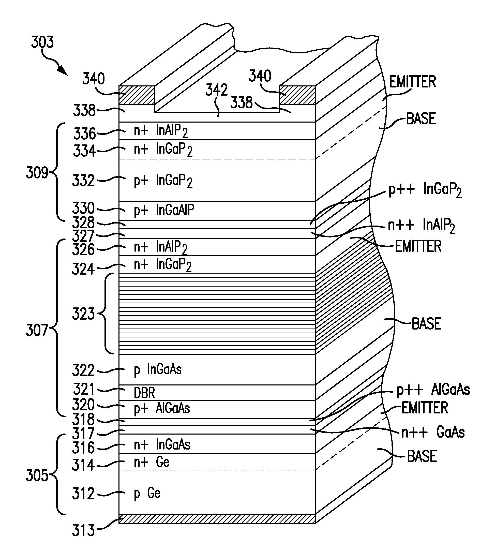
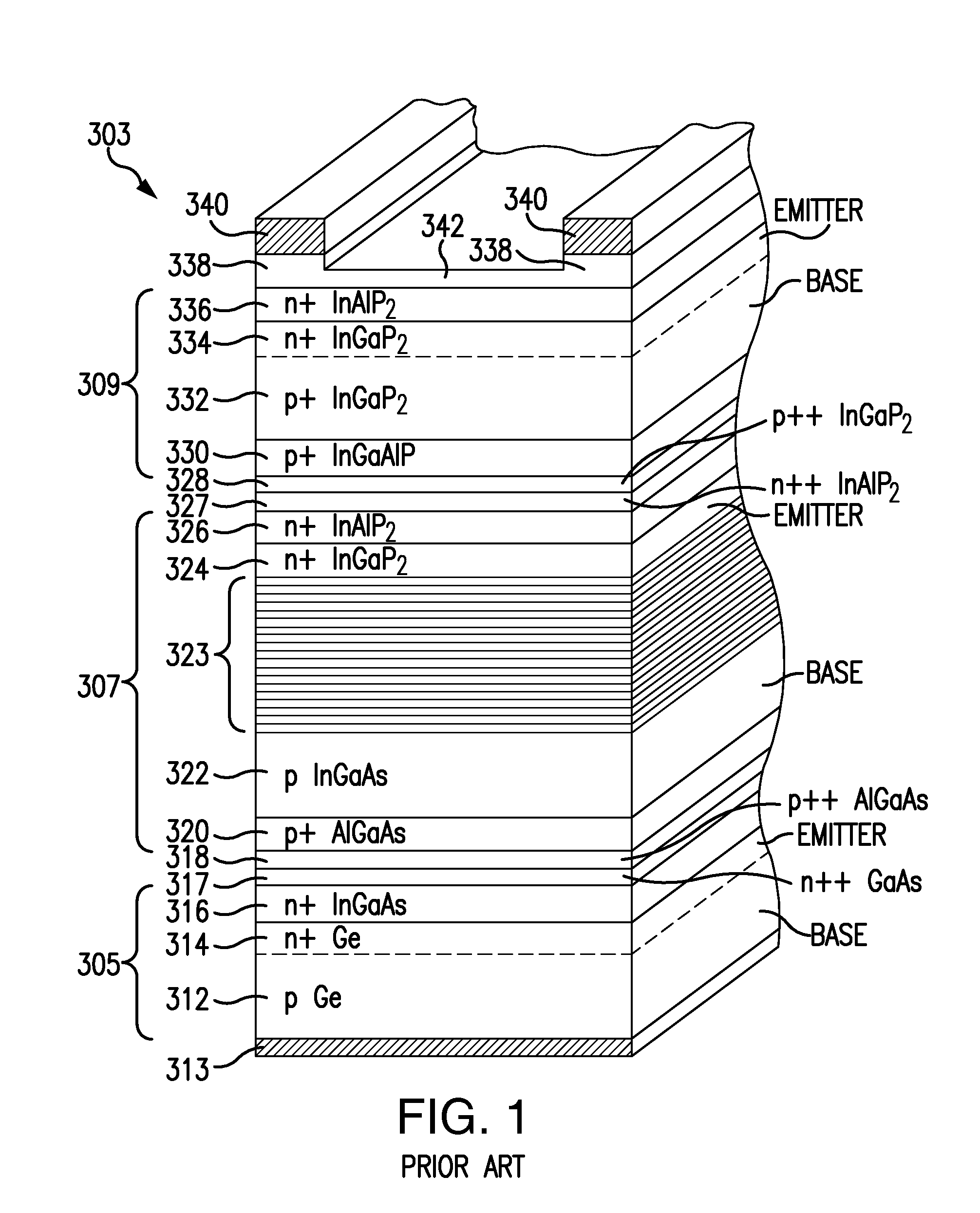
[0072]FIG. 3 illustrates a multijunction solar cell device 303 in which the middle subcell 307 has been modified in order to provide an increase in the overall multijunction cell efficiency. As shown in FIG. 3, the bottom subcell 305 includes a substrate 312 and other layers 314, 316, 316, 317 and 318 which are identical to those described in FIG. 1, and therefore the description of such layers will not be repeated here.

[0073]In the illustrated example of FIG. 3, the middle subcell 307 includes a highly doped p-type aluminum gallium arsenide (“AlGaAs”) back surface field (“BSF”) layer 320. On top of the back surface field (“BSF”) layer 320 is a distributed Bragg reflector layer 321. In this first embodiment of the present disclosure, a distributed Bragg reflector (“DBR”) layer 321 is formed in the base layer of the middle subcell, and is constituted by alternating layers of semiconductor materials with different refractive indices but closely lattice matched to the substrate, such a...

second embodiment

[0078]FIG. 4 is a multijunction solar cell according to the present disclosure. As shown in FIG. 5, the bottom subcell 305 includes a substrate 312 and other layers 314, 316, 317 and 318 which are identical to those described in FIG. 1, and therefore the description of such layers will not be repeated here.

[0079]In the illustrated example of FIG. 4, the middle subcell 307 includes a highly doped p-type aluminum gallium arsenide (“AlGaAs”) back surface field (“BSF”) layer 320. Below the back surface field (“BSF”) layer 320 is a distributed Bragg reflector layer 321, which is formed directly over the tunnel diode 317 / 318. In this second embodiment of the present disclosure, a distributed Bragg reflector (“DBR”) layer 321 is substantially identical to that described in connection with FIG. 3, and thus the description of the DBR layers will not be repeated here.

[0080]In the illustrated example of FIG. 5, a highly doped p-type aluminum gallium arsenide (“AlGaAs”) back surface field (“BSF...

third embodiment

[0082]FIG. 5 is a multijunction solar cell according to the present disclosure. As shown in FIG. 5, the bottom subcell 305 includes a substrate 312 and other layers 314 and 316 which are identical to those described in FIG. 1, and therefore the description of such layers will not be repeated here.

[0083]In the embodiment of FIG. 5, a distributed Bragg reflector (“DBR”) layer 319 is deposited directly on top of the nucleation layer 316. The DBR layer 319 is substantially identical to that described in connection with FIG. 4, and thus the description of the DBR layers will not be repeated here.

[0084]Heavily doped p-type aluminum gallium arsenide (“AlGaAs”) and heavily doped n-type gallium arsenide (“GaAs”) tunneling junction layers 318, 317 may be deposited over the DBR layer 319 to provide a low resistance pathway between the bottom and middle subcells.

[0085]In the illustrated example of FIG. 5, the middle subcell 307 includes a highly doped p-type aluminum gallium arsenide (“AlGaAs”)...


PUM


Abstract

A multijunction photovoltaic cell including a top subcell; a second subcell disposed immediately adjacent to the top subcell and producing a first photo-generated current; and including a sequence of first and second different semiconductor layers with different lattice constant; and a lower subcell disposed immediately adjacent to the second subcell and producing a second photo-generated current substantially equal in amount to the first photo-generated current density.

Description

GOVERNMENT RIGHTS STATEMENT[0001]This invention was made with government support under Contract No. NRO 000-10-C-0285. The Government has certain rights in the invention.BACKGROUND OF THE INVENTION[0002]1. Field of the Invention[0003]The present disclosure relates to solar cells and the fabrication of solar cells, and more particularly the design and specification of the middle cell in multijunction solar cells based on III-V semiconductor compounds.[0004]2. Description of the Related Art[0005]Solar power from photovoltaic cells, also called solar cells, has been predominantly provided by silicon semiconductor technology. In the past several years, however, high-volume manufacturing of III-V compound semiconductor multijunction solar cells for space applications has accelerated the development of such technology not only for use in space but also for terrestrial solar power applications. Compared to silicon, III-V compound semiconductor multijunction devices have greater energy conv...

Claims


Application Information

Patent Timeline
Patent Type & Authority Applications(United States)
IPC IPC(8): H01L31/0304H01L31/18H01L31/0725
CPCH01L31/035236H01L31/075H01L31/078H01L31/1852H01L31/0725H01L31/18B82Y20/00Y02E10/52Y02E10/544Y02E10/548Y02P70/50
Inventor RICHARDS, BENJAMIN C.LIN, YONGSHARPS, PAUL R.PATEL, PRAVIN
Owner SOLAERO TECH CORP
Why Eureka
Try Eureka