Polymer/inorganic multi-layer encapsulation film
- Summary
- Abstract
- Description
- Claims
- Application Information
AI Technical Summary
Benefits of technology
Problems solved by technology
Method used
Image
Examples
example 1
Formation of Inorganic Thin Film Layer using Atomic Layer Deposition
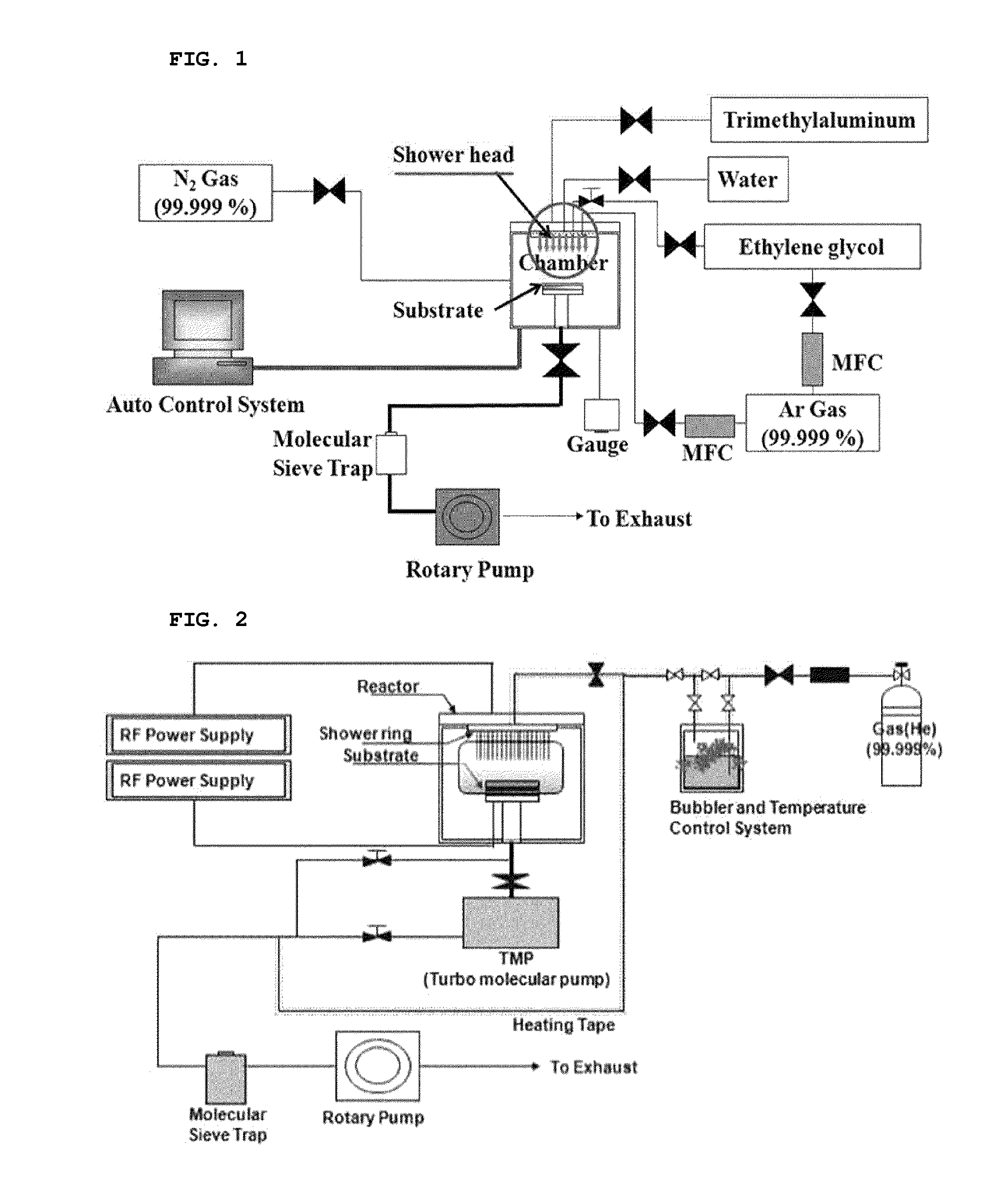
[0060]An inorganic thin film layer was formed by performing atomic layer deposition using an apparatus illustrated in FIG. 1. As such, a vacuum chamber was maintained at 500 mTorr, and trimethyl aluminum and H2O were injected via a difference in pressure from the chamber, thus forming an Al2O3 inorganic thin film. In order to accomplish uniform deposition on the entire surface of polyethylene naphthalate (PEN) used as a plastic substrate, the temperature of the substrate was maintained at 85° C., and thus thermal energy suitable for a chemical reaction was supplied. Furthermore, the injection time of the inorganic material and the purging time of the remaining gas were adjusted, whereby the process conditions (TMA 1 sec—purge 15 sec—H2O 1 sec—purge 15 sec; 1 cycle) were determined. Through one cycle process, a thin film having a thickness of 0.12 nm was deposited, and 200 processes were repeated, thus manufacturing ...
example 2
Formation of Plasma polymer Thin Film Layer using PECVD
[0061]A plasma polymer thin film layer was formed using a PECVD (Plasma Enhanced Chemical Vapor Deposition) apparatus illustrated in FIG. 2. A plasma polymer thin film deposition process was implemented by means of a process chamber having a chamber lid at the top thereof and a chamber body at the bottom thereof. Used as the precursor of the plasma polymer thin film was tetrakis(trimethylsilyloxy)silane (TTMSS). This precursor was used as a reactive gas, and the reactive gas was uniformly sprayed onto a substrate placed on a substrate susceptor in the chamber body by means of a shower ring provided at the chamber lid maintained at 200 mTorr, thus depositing a thin film. The temperature of 88° C. or higher was maintained so that TTMSS used as the reactive gas was emitted in a vapor state from a bubbler, and the temperature of the line was maintained at 99° C. in order to keep the vapor state even in the line connected up to the c...
example 3
Measurement of Moisture and Oxygen Permeability of Multi-Layer Encapsulation Film According to the Present Invention
[0062]The multi-layer encapsulation film manufactured by the method of forming the inorganic thin film layer in Example 1 and the method of forming the plasma polymer thin film layer in Example 2 was measured for moisture and oxygen permeability using Ca-test.
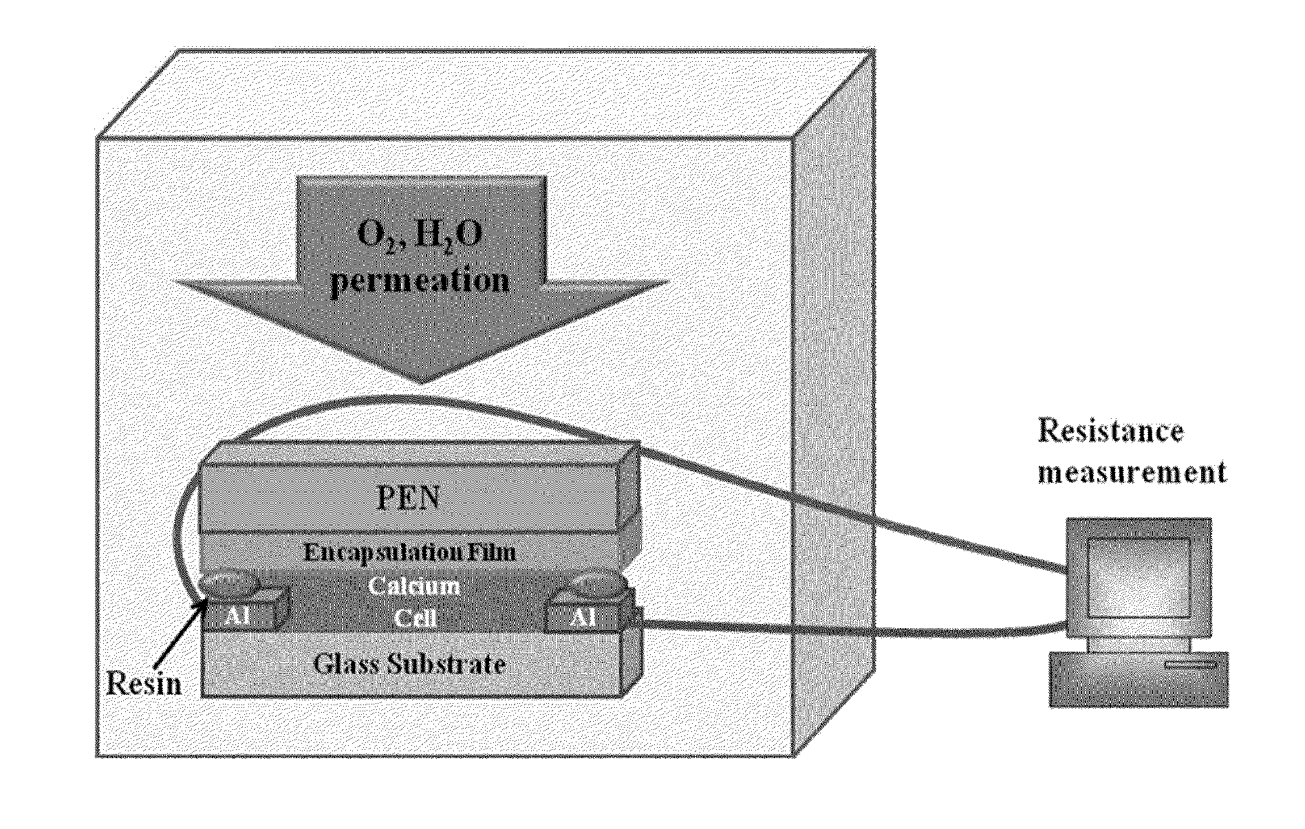
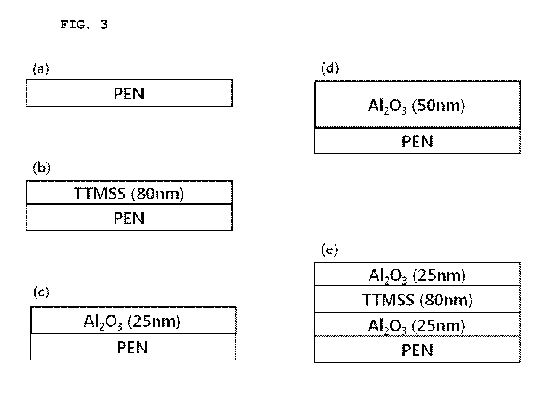
[0063]A variety of films are shown in FIG. 3. FIG. 3(b) illustrates a PEN substrate having a 80 nm thick TTMSS polymer layer deposited thereon, FIG. 3(c) illustrates a PEN substrate having a 25 nm thick Al2O3 layer deposited thereon, FIG. 3(d) illustrates a PEN substrate having a 50 nm thick Al2O3 layer deposited thereon, and FIG. 3(e) illustrates a PEN substrate having a 25 nm thick Al2O3 layer / a 80 nm thick TTMSS polymer layer / a 25 nm Al2O3 layer deposited thereon. The encapsulation properties of these substrates were compared and analyzed using Ca-test equipment illustrated in FIG. 4.
[0064]150 nm thick Al was d...
PUM
| Property | Measurement | Unit |
|---|---|---|
| Thickness | aaaaa | aaaaa |
| Thickness | aaaaa | aaaaa |
| Flexibility | aaaaa | aaaaa |
Abstract
Description
Claims
Application Information


