Nanoelectromechanical resonators

a nano-electromechanical and resonator technology, applied in the field of resonators, can solve the problems of inability to manufacture and integrate devices as single-chip solutions in mass sensing or signal processing applications, inability to predict device design, and inability to achieve near-resonant response characteristics that are not easily reproduced and other problems, to achieve the effect of effective and economical manufacturing

Inactive Publication Date: 2014-07-24
PURDUE RES FOUND INC
View PDF11 Cites 10 Cited by
  • Summary
  • Abstract
  • Description
  • Claims
  • Application Information

AI Technical Summary

Benefits of technology

[0007]There is therefore a need for a CMOS compatible processing technique to permit effectively and economically manufacturing NEMS devices, and in particular NEMS-based resonators, mass sensing devices, and signal processing components. There is also a need for such devices fabricated on-chip with CMOS electronics.

Problems solved by technology

While this approach can be adopted for post-CMOS device fabrication, it is quite susceptible to processing, material, and geometric variability, which leads to irreproducible near-resonant response characteristics and, ultimately, prohibits predictive device design.
However, these devices generally cannot be fabricated and integrated as a single-chip solution in mass sensing or signal processing applications, as technologies that are not based on Si resonators are generally incompatible with CMOS processing, and devices which rely on piezoelectric, magnetomotive, or optical transduction typically require additional hardware to fully characterize their near-resonant response.

Method used


Image

  • Nanoelectromechanical resonators
  • Nanoelectromechanical resonators
  • Nanoelectromechanical resonators

Examples


Embodiment Construction

[0048]For the purposes of promoting an understanding of the principles of the present disclosure, reference will now be made to the embodiments illustrated in the drawings, and specific language will be used to describe the same. It will nevertheless be understood that no limitation of the scope of this disclosure is thereby intended.

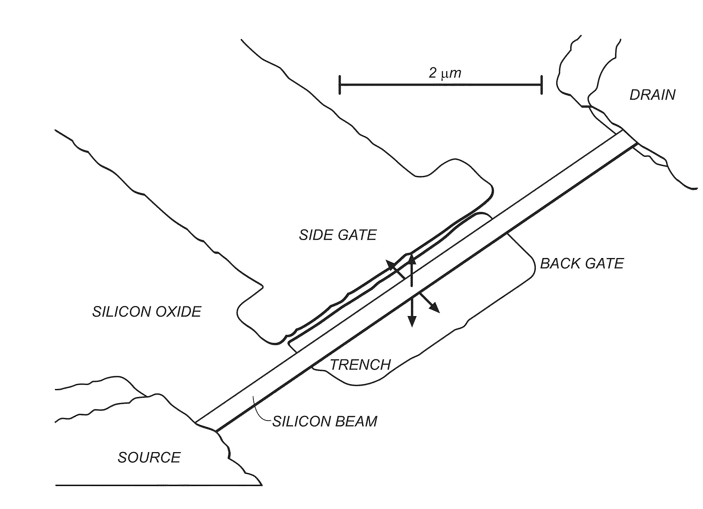
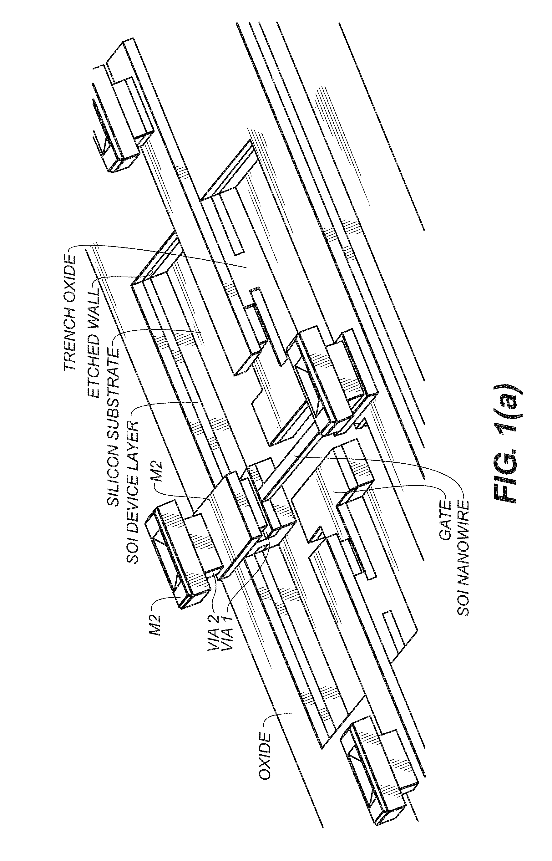
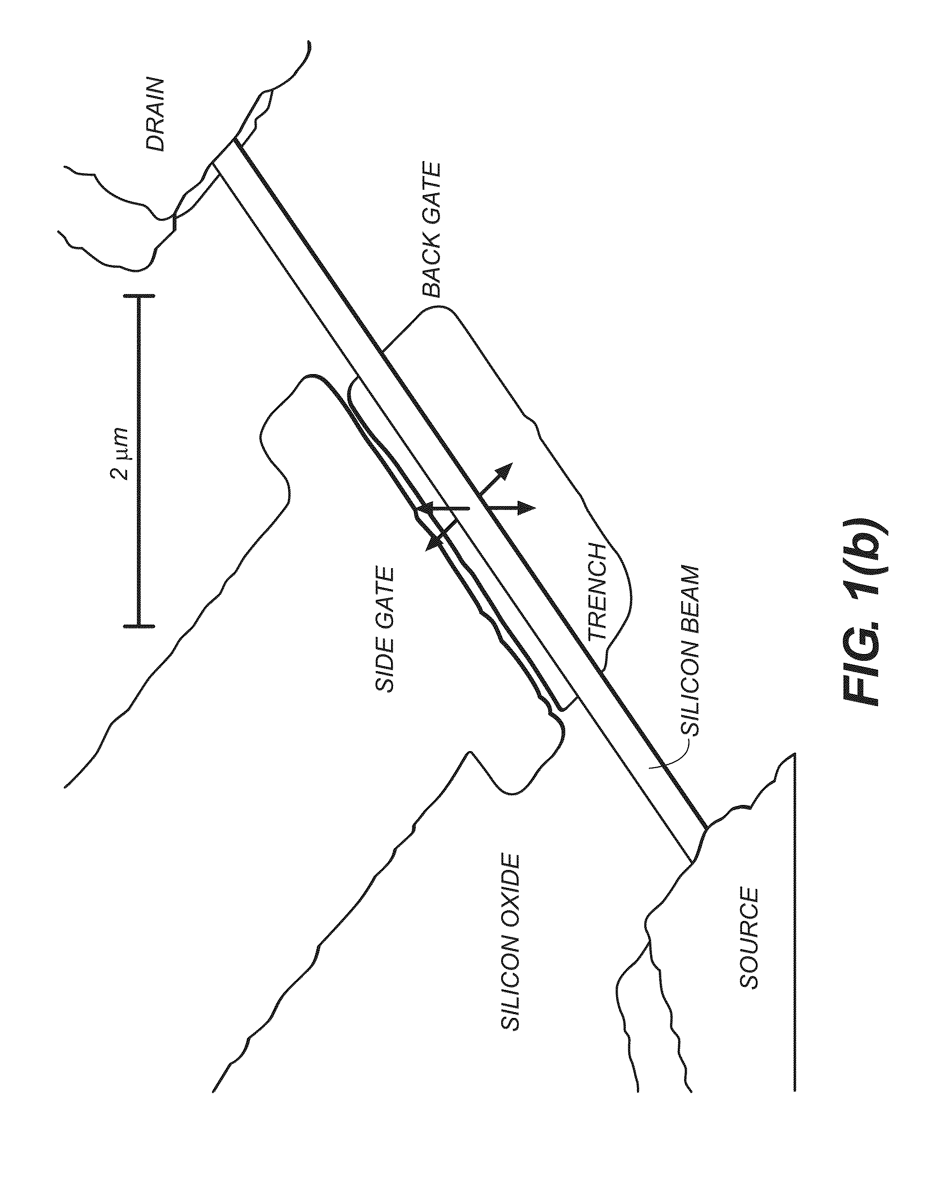
[0049]The present disclosure provides a method for design, development, and characterization of electrostatically-transduced nanoelectromechanical resonators using a top-down microfabrication technique, using a silicon-on-insulator (SOI) process flow. SOI-complementary metal oxide semiconductor (CMOS) technology is widely employed in the development of low-power digital microprocessors, such as those used in mobile computing and communication platforms. The selective nature of silicon / silicon dioxide (Si / SiO2) etching which enables the fabrication of these devices also allows for the development, implementation, and on-chip integration of SOI-NEMS. Thes...


PUM


Abstract

A silicon device, e.g., a nanoelectromechanical resonator, has a silicon substrate; an oxide layer having a trench therein; a silicon device layer over the oxide layer; and a nanowire disposed at least partly over the trench. Substantially no oxide or polysilicon is over the nanowire in the trench. A polyimide layer over the silicon device layer includes an opening over the trench. A silicon device can include silicon-on-insulator layers and at least one complementary metal-oxide semiconductor transistor in addition to a nanowire substantially suspended over a trench. A system for measurement of a nanoresonator includes an AC source in series with the nanoresonator to provide an electrical signal thereto at a selected first frequency. Electrode(s) adjacent to and spaced apart from the nanoresonator are driven by voltage source. A detector detects a current through the nanoresonator.

Description

CROSS-REFERENCE TO RELATED APPLICATIONS[0001]This application is a nonprovisional application of U.S. Patent Application Ser. No. 61 / 684,259, filed Aug. 17, 2012 and entitled “Nanoelectromechanical Resonators,” the entirety of which is incorporated herein by reference.STATEMENT OF FEDERALLY SPONSORED RESEARCH OR DEVELOPMENT[0002]This invention was made with government support under grant number 0826276 awarded by the National Science Foundation. The government has certain rights in the invention.TECHNICAL FIELD[0003]The present disclosure generally relates to micro- and nano-electromechanical systems, and in particular to resonators in such systems.BACKGROUND[0004]Nanoelectromechanical systems (NEMS) are eliciting great interest in various electronic fields. In one such field NEMS have received interests because these devices allow access to microwave frequencies and nanosecond response times, amongst other pertinent metrics. These properties permit NEMS to be useful in analog and r...

Claims


Application Information

Patent Timeline
Patent Type & Authority Applications(United States)
IPC IPC(8): H01L27/12G01R19/00H01L29/02
CPCH01L27/1203G01R19/0015H01L29/02H03H3/0072H03H3/0073H03H9/02409H03H9/2463H03H2009/02314B82Y10/00B82Y15/00H01L29/775H01L29/0673H01L29/16
Inventor MOHAMMADI, SAEEDPAJOUHI, HOSSEINRHOADS, JEFFREY FREDERICKYU, LIN
Owner PURDUE RES FOUND INC
Why Eureka
Try Eureka