Laser and plasma etch wafer dicing with etch chamber shield ring for film frame wafer applications

a technology of shield rings and etch chambers, applied in the field of semiconductor wafer dicing, can solve the problems of chip and gouges along the severed edges of dice, inoperable integrated circuits, cracks and propagation,

Active Publication Date: 2014-07-31
APPLIED MATERIALS INC
View PDF3 Cites 36 Cited by
  • Summary
  • Abstract
  • Description
  • Claims
  • Application Information

AI Technical Summary

Problems solved by technology

One problem with either scribing or sawing is that chips and gouges can form along the severed edges of the dice.
In addition, cracks can form and propagate from the edges of the dice into the substrate and render the integrated circuit inoperative.
Chipping and cracking are particularly a problem with scribing because only one side of a square or rectangular die can be scribed in the direction of the crystalline structure.
Consequently, cleaving of the other side of the die results in a jagged separation line.
As a result of the spacing requirements, not as many dice can be formed on a standard sized wafer and wafer real estate that could otherwise be used for circuitry is wasted.
Furthermore, after cutting, each die requires substantial cleaning to remove particles and other contaminants that result from the sawing process.
Plasma dicing has also been used, but may have limitations as well.
For example, one limitation hampering implementation of plasma dicing may be cost.
A standard lithography operation for patterning resist may render implementation cost prohibitive.
Another limitation possibly hampering implementation of plasma dicing is that plasma processing of commonly encountered metals (e.g., copper) in dicing along streets can create production issues or throughput limits.

Method used


Image

  • Laser and plasma etch wafer dicing with etch chamber shield ring for film frame wafer applications
  • Laser and plasma etch wafer dicing with etch chamber shield ring for film frame wafer applications
  • Laser and plasma etch wafer dicing with etch chamber shield ring for film frame wafer applications

Examples


Embodiment Construction

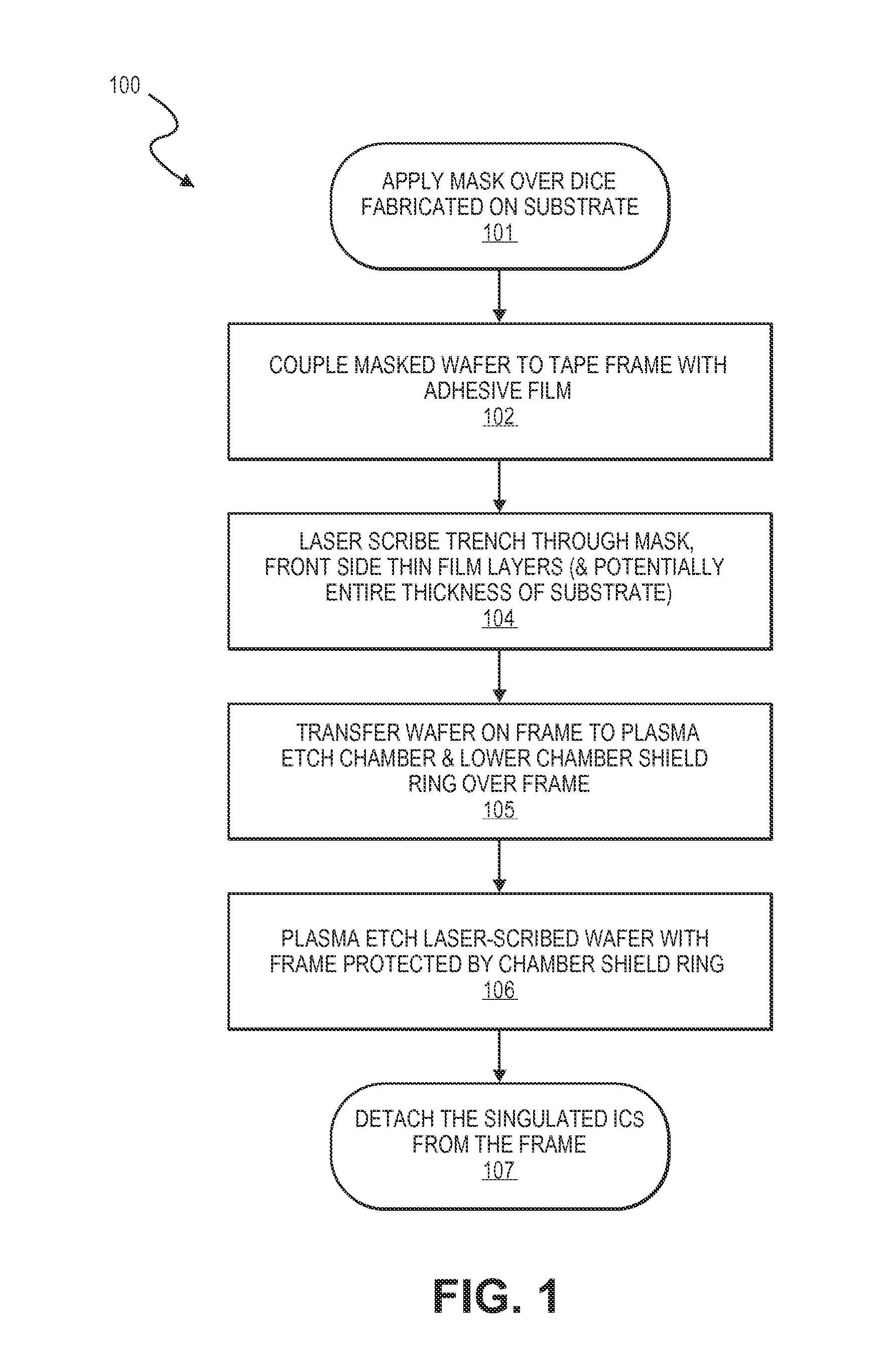
[0021]Methods of dicing semiconductor wafers, each wafer having a plurality of integrated circuits thereon, are described. In the following description, numerous specific details are set forth, such as laser and plasma etch wafer dicing approaches with temperature control hardware and techniques, in order to provide a thorough understanding of embodiments of the present invention. It will be apparent to one skilled in the art that embodiments of the present invention may be practiced without these specific details. In other instances, well-known aspects, such as integrated circuit fabrication, are not described in detail in order to not unnecessarily obscure embodiments of the present invention. Furthermore, it is to be understood that the various embodiments shown in the Figures are illustrative representations and are not necessarily drawn to scale.

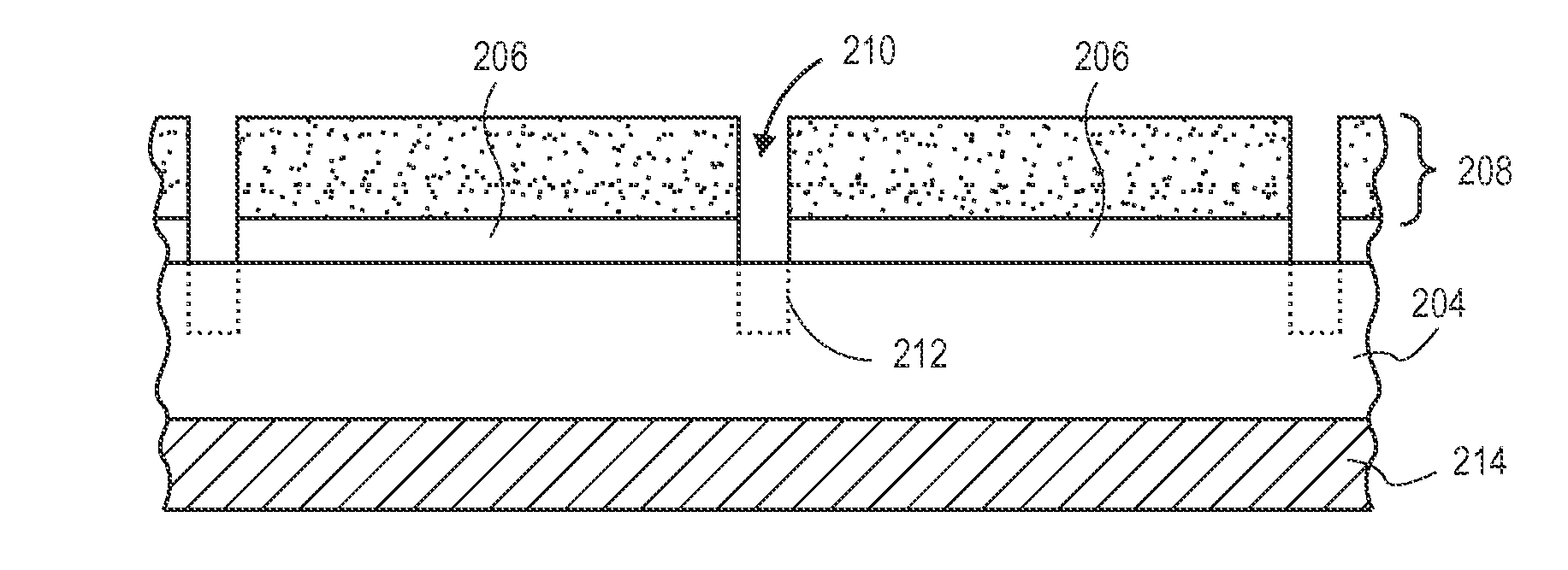
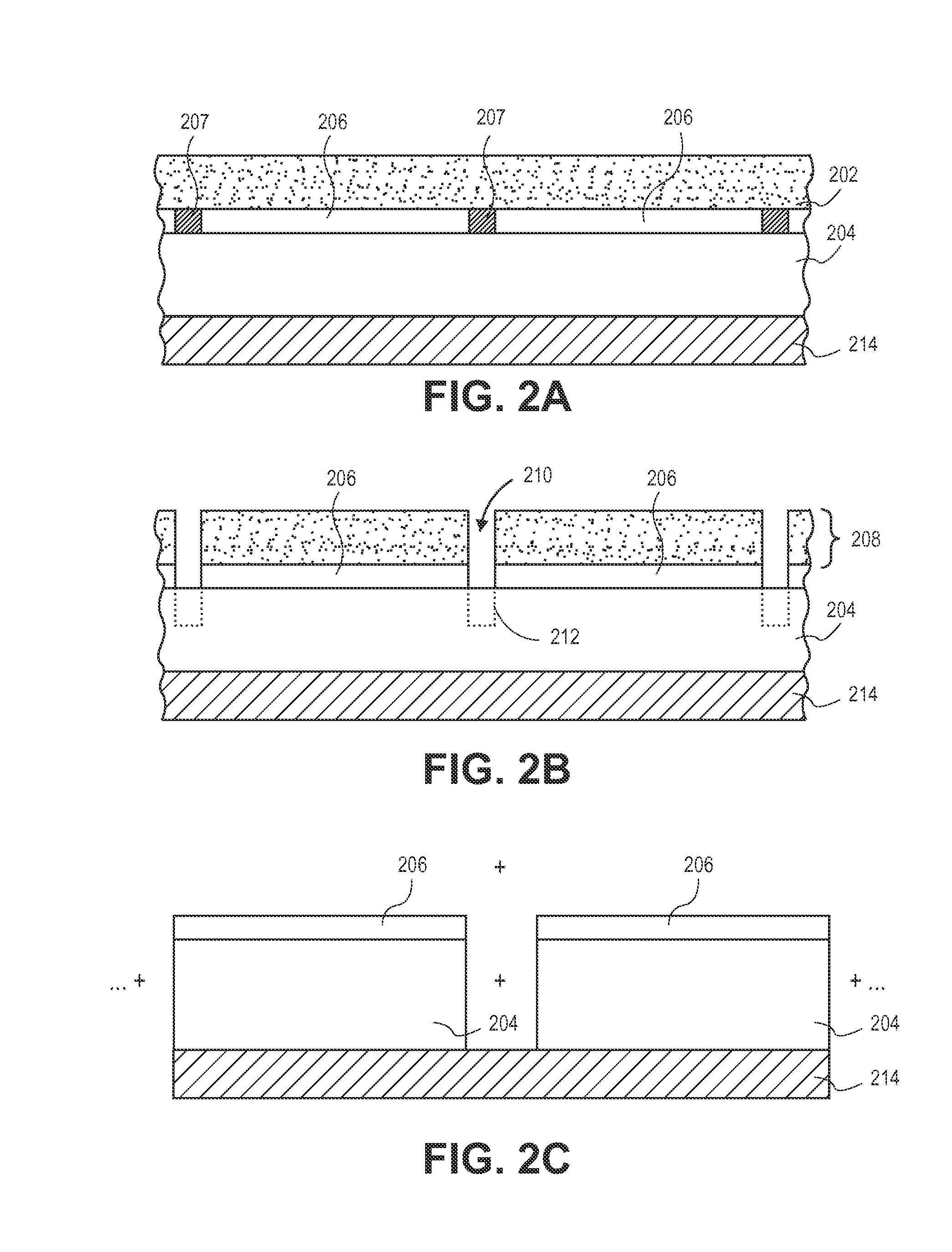
[0022]A hybrid wafer or substrate dicing process involving an initial laser scribe and subsequent plasma etch may be implemented for d...


PUM

PropertyMeasurementUnit
temperatureaaaaaaaaaa
diameteraaaaaaaaaa
diameteraaaaaaaaaa

Abstract

Laser and plasma etch wafer dicing where a mask is formed covering ICs formed on the wafer, as well as any bumps providing an interface to the ICs. The semiconductor wafer is coupled to a film frame by an adhesive film. The mask is patterned by laser scribing to provide a patterned mask with gaps. The laser scribing exposes regions of the semiconductor wafer, below thin film layers from which the ICs are formed. The semiconductor wafer is plasma etched through the gaps in the patterned mask while the film frame is maintained at an acceptably low temperature with a chamber shield ring configured to sit beyond the wafer edge and cover the frame. The shield ring may be raised and lowered, for example, on lifter pins to facilitate transfer of the wafer on frame.

Description

PRIORITY[0001]This application is a Non-Provisional of, claims priority to, and incorporates by reference in its entirety for all purposes, the U.S. Provisional Patent Application No. 61 / 757,031 filed Jan. 25, 2013.TECHNICAL FIELD[0002]Embodiments of the present invention pertain to the field of semiconductor processing and, in particular, to methods of dicing semiconductor wafers, each wafer having a plurality of integrated circuits thereon.DESCRIPTION OF RELATED ART[0003]In semiconductor wafer processing, integrated circuits are formed on a wafer (also referred to as a substrate) composed of silicon or other semiconductor material. In general, layers of various materials which are either semiconducting, conducting, or insulating are utilized to form the integrated circuits. These materials are deposited and etched using various well-known processes to form integrated circuits. Each wafer is processed to form a large number of individual regions containing integrated circuits known...

Claims


Application Information

Patent Timeline
Patent Type & Authority Applications(United States)
IPC IPC(8): H01L21/78H01L21/3065H01L21/308H01L21/027
CPCH01L21/78H01L21/3065H01L21/0271H01L2221/68327H01L21/31127H01J37/32009H01L21/6836H01L21/31105B23K26/40B23K26/364B23K2103/172B23K2103/50H01L2221/68318H01L2221/68381B23K26/402
Inventor LEI, WEI-SHENGSINGH, SARAVJEETDINEV, JIVKOIYER, APARNAEATON, BRADKUMAR, AJAY
Owner APPLIED MATERIALS INC
Why Eureka
Try Eureka