Semiconductor device and method of manufacturing the same

a semiconductor and semiconductor technology, applied in the direction of semiconductor devices, basic electric elements, electrical equipment, etc., can solve the problems of increasing the conduction loss, high cost, and high cost of the method of patent document 3 and other problems, to achieve the effect of improving the trade-off relationship, and reducing the cos

Inactive Publication Date: 2014-08-14
FUJI ELECTRIC CO LTD
View PDF1 Cites 6 Cited by
  • Summary
  • Abstract
  • Description
  • Claims
  • Application Information

AI Technical Summary

Benefits of technology

[0048]The present invention as stated above provides a semiconductor device that improves the trade-off relationship between the Eoff and the turning OFF dV / dt by forming a high concentration n type semiconductor region in the upper portion of an n type layer of the parallel pn layer, the impurity concentration of the region being higher at the p type layer side than at the center of the n type layer.
[0049]The present invention as stated above provides a method for manufacturing a semiconductor device that improves the trade-off relationship between the Eoff and the turning OFF dV / dt by forming a parallel pn layer having a superjunction structure employing a trench embedding method, and conducting ion implantation process into the upper portion of an n type semiconductor layer, i.e. an n type column, to form a high concentration n type semiconductor region.
[0050]Because the redundant repeating of steps as in the conventional multi-stage epitaxial growth method has been eliminated, the procedure has been shortened and the manufacturing costs has been reduced in the method of the invention.

Problems solved by technology

Conversely, a semiconductor device exhibiting a high withstand voltage with a thick n− drift layer has a large ON resistance and increases a conduction loss.
This procedure needs multiple steps and high cost.
Because the epitaxial growth method is employed for forming the high concentration n type semiconductor layer, the method of Patent Document 3 is costly.

Method used


Image

  • Semiconductor device and method of manufacturing the same
  • Semiconductor device and method of manufacturing the same
  • Semiconductor device and method of manufacturing the same

Examples


embodiment example 1

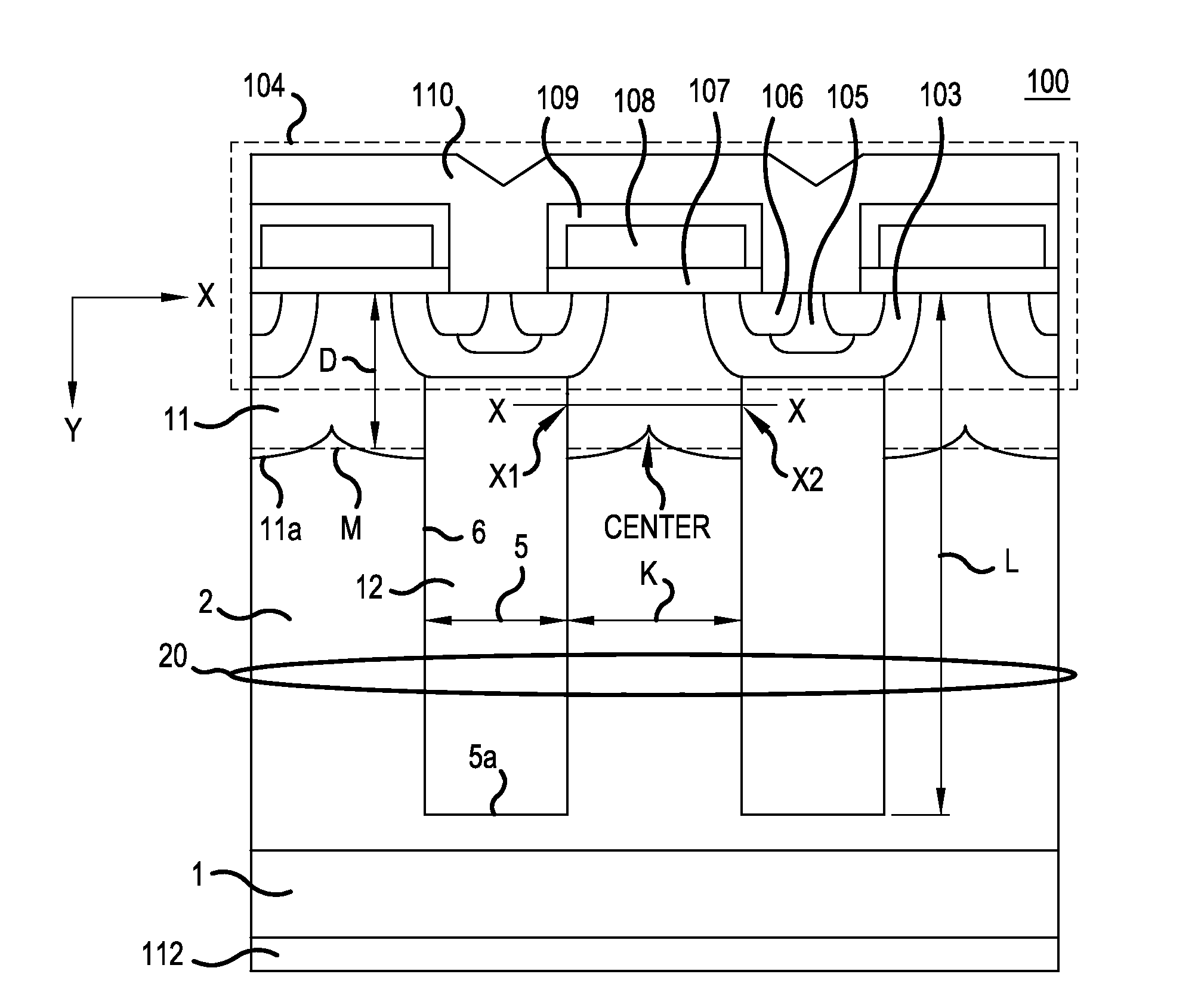
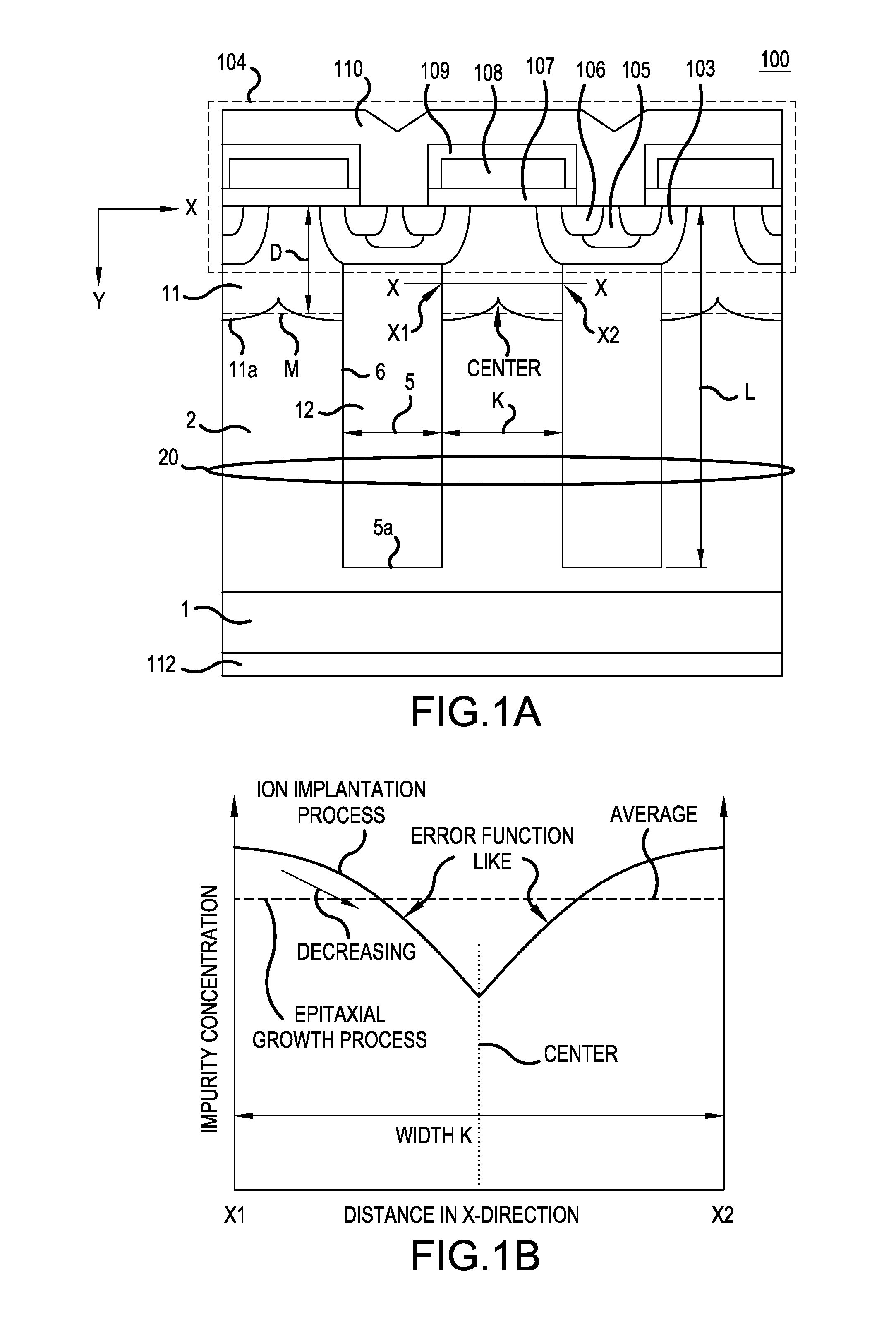
[0077]FIGS. 1A and 1B are drawings for explaining semiconductor device 100 according to an Embodiment Example 1 of the present invention, wherein FIG. 1A is a sectional view of an essential part of semiconductor device 100 and FIG. 1B is a graph showing a profile of impurity concentration along a lateral direction in a high concentration n type semiconductor region. The semiconductor device of FIG. 1A is an example of a superjunction (SJ) MOSFET. The ordinate of FIG. 1B represents an impurity concentration in a logarithmic scale.

[0078]Device surface structure 104 is formed on a first principal surface, which is a top surface of parallel pn layer 20, of semiconductor device 100. The device surface structure comprises: p base region 103, p+ contact region 105, and n+ source region 106. Gate electrode 108 is formed through gate insulation film 107 on the surface of p base region 103 between n type semiconductor layer 2 and n+ source region 106. Interlayer dielectric film 109 is formed ...

embodiment example 2

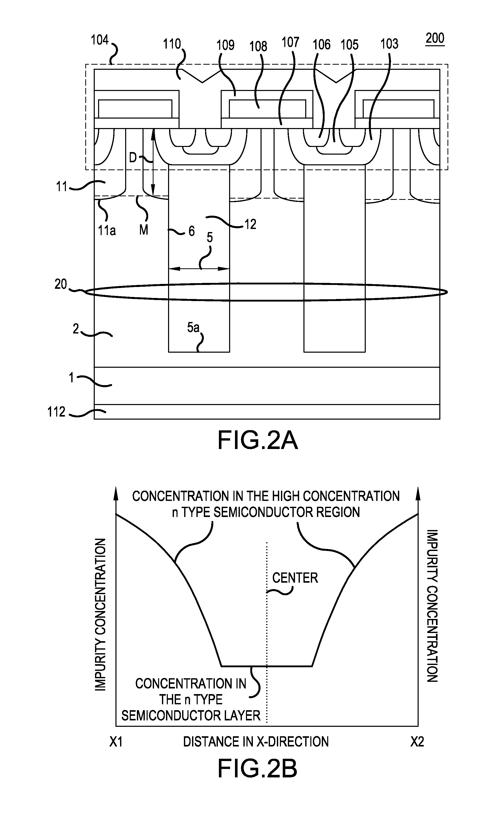
[0087]FIGS. 2A and 2B illustrate semiconductor device 200 according to Embodiment Example 2 of the present invention, wherein FIG. 2A is a sectional view of an essential part of semiconductor device 200 and FIG. 2B is an impurity concentration profile along the lateral direction in the high concentration n type semiconductor region. The ordinate of FIG. 2B represents the impurity concentration in a logarithmic scale.

[0088]The semiconductor device of FIGS. 2A and 2B is different from the device of FIGS. 1A and 1B in that the device of FIGS. 2A and 2B lacks a central part of high concentration n type semiconductor region 11. This construction also has the same effects as the construction of FIGS. 1A and 1B. In this construction, a heat treatment step for forming high concentration n type semiconductor region 11 can be conducted after embedding p type semiconductor layer 12 into trench 5. This heat treatment process can be carried out, at the same time as a heat treatment process for f...

embodiment example 3

[0089]FIGS. 3 through 11 are sectional views of an essential part of a semiconductor device in the method of manufacturing the semiconductor device according to Embodiment Example 3 of the present invention showing in the sequence of manufacturing steps.

[0090](1) First, as shown in FIG. 3, on n type semiconductor substrate 1, which can be a silicon substrate and becomes a high concentration n type drain layer, n type semiconductor layer 2a, which can be a silicon layer, is formed by epitaxial growth to a thickness of about 45 μm, for example. Then oxide layer 3a, which can be SiO2, is formed on n type semiconductor layer 2a.

[0091](2) Then, as shown in FIG. 4, oxide film 3 having openings 4a is formed by patterning oxide film 3a using a photo-lithography technique. The planar pattern here is for example, a line-and-space configuration with an opening width W of 6 μm and a repetition pitch T (indicated in FIG. 6), i.e., an SJ pitch, of 12 μm. The line-and-space configuration is, as s...


PUM

PropertyMeasurementUnit
aspect ratioaaaaaaaaaa
thicknessaaaaaaaaaa
widthaaaaaaaaaa

Abstract

A semiconductor device and method of manufacturing the semiconductor device is disclosed in which the tradeoff relationship between the Eoff and the turning OFF dV/dt is improved at a low cost using a trench embedding method. The method comprises a step of forming a parallel pn layer that is a superjunction structure using a trench embedding method and a step of ion implantation into an upper part of an n type semiconductor layer, i.e., an n type column, forming a high concentration n type semiconductor region. This method improves the trade-off relationship between the Eoff and the turning OFF dV/dt as compared with a high concentration n type semiconductor region formed of an epitaxial layer. This method achieves shorter process time and lower cost in manufacturing because it eliminates the redundant repeating of steps performed in the conventional method of forming a superjunction structure through multi-stage epitaxial growth.

Description

CROSS-REFERENCE TO RELATED APPLICATION[0001]This application is based on, and claims priority to, Japanese Patent Application No. 2013-026592, filed on Feb. 14, 2013, contents of which are incorporated herein by reference.BACKGROUND OF THE INVENTION[0002]A. Field of the Invention[0003]The present invention relates to a power semiconductor device such as a MOSFET, and in particular, to a semiconductor device and a method of manufacturing the semiconductor device that has a drift layer with a superjunction structure, or a parallel pn column structure or parallel pn layer structure. The superjunction structure comprises an n type column and a p type column alternately adjoining each other and extending in a vertical direction with respect to a principal surface of a semiconductor substrate.[0004]B. Description of the Related Art[0005]Semiconductor devices are generally classified into lateral devices having electrodes formed on one surface of a semiconductor substrate and vertical devi...

Claims


Application Information

Patent Timeline
Patent Type & Authority Applications(United States)
IPC IPC(8): H01L21/02H01L29/06
CPCH01L29/0688H01L21/02658H01L29/0634H01L29/66712H01L29/7802H01L21/26586H01L29/0878H01L29/1095
Inventor KITAMURA, MUTSUMIYAMADA, MICHIYAFUJIHIRA, TATSUHIKO
Owner FUJI ELECTRIC CO LTD
Why Eureka
Try Eureka